MAX4411ETP+ Maxim Integrated Products, MAX4411ETP+ Datasheet - Page 12
MAX4411ETP+
Manufacturer Part Number
MAX4411ETP+
Description
IC AMP AUDIO .08W STER AB 20TQFN
Manufacturer
Maxim Integrated Products
Series
DirectDrive™r
Type
Class ABr
Datasheet
1.MAX4411EBET.pdf
(18 pages)
Specifications of MAX4411ETP+
Output Type
Headphones, 2-Channel (Stereo)
Max Output Power X Channels @ Load
80mW x 2 @ 16 Ohm
Voltage - Supply
1.8 V ~ 3.6 V
Features
Depop, Short-Circuit and Thermal Protection, Shutdown
Mounting Type
Surface Mount
Package / Case
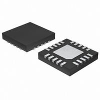
20-TQFN Exposed Pad
Product
General Purpose Audio Amplifiers
Output Power
80 mW
Thd Plus Noise
0.007 %
Operating Supply Voltage
1.8 V to 3.6 V
Supply Current
3.2 mA
Maximum Power Dissipation
1349 mW
Maximum Operating Temperature
+ 85 C
Mounting Style
SMD/SMT
Minimum Operating Temperature
- 40 C
Supply Voltage (max)
3.6 V
Supply Voltage (min)
1.8 V
Amplifier Class
AB
No. Of Channels
2
Supply Voltage Range
1.8V To 3.6V
Load Impedance
16ohm
Operating Temperature Range
-40°C To +85°C
Amplifier Case Style
TQFN
Rohs Compliant
Yes
Lead Free Status / RoHS Status
Lead free / RoHS Compliant


80mW, Fixed-Gain, DirectDrive, Stereo
Headphone Amplifier with Shutdown
output, supply, and ground traces improve the maxi-
mum power dissipation in the package.
Thermal-overload protection limits total power dissipa-
tion in the MAX4411. When the junction temperature
exceeds +140°C, the thermal protection circuitry dis-
ables the amplifier output stage. The amplifiers are
enabled once the junction temperature cools by 15°C.
This results in a pulsing output under continuous thermal-
overload conditions.
The device has been specified for the worst-case sce-
nario—when both inputs are in phase. Under this con-
dition, the drivers simultaneously draw current from the
charge pump, leading to a slight loss in headroom of
V
right signals have differences in both magnitude and
phase, subsequently leading to an increase in the max-
imum attainable output power. Figure 5 shows the two
extreme cases for in and out of phase. In reality, the
available power lies between these extremes.
An additional benefit of the MAX4411 is the internally
generated, negative supply voltage (PV
age provides the ground-referenced output level. PV
can, however, also be used to power other devices
within a design limit current drawn from PV
exceeding this affects the headphone driver operation.
A typical application is a negative supply to adjust the
contrast of LCD modules.
Figure 5. Output Power vs. Supply Voltage with Inputs In/Out of
Phase
12
SS
. In typical stereo audio applications, the left and
______________________________________________________________________________________
300
250
200
150
100
50
0
1.8
OUTPUT POWER vs. SUPPLY VOLTAGE
Powering Other Circuits from a
f
R
THD+N = 10%
IN
L
= 1kHz
= 16Ω
2.1
SUPPLY VOLTAGE (V)
2.4
2.7
OUT OF PHASE
INPUTS 180°
3.0
Negative Supply
IN PHASE
INPUTS
3.3
Output Power
SS
). This volt-
3.6
SS
to 5mA;
SS
PV
lated voltage. The charge-pump output impedance
must be taken into account when powering other
devices from PV
ance plot appears in the Typical Operating
Characteristics. For best results, use 2.2µF charge-
pump capacitors.
The input capacitor (C
nal R
bias from an incoming signal (see Typical Application
Circuit). The AC-coupling capacitor allows the amplifier
to bias the signal to an optimum DC level. Assuming
zero-source impedance, the -3dB point of the highpass
filter is given by:
R
given in the Electrical Characteristics. Choose the C
such that f
interest. Setting f
frequency response. Use capacitors whose dielectrics
have low-voltage coefficients, such as tantalum or
aluminum electrolytic ones. Capacitors with high-voltage
coefficients, such as ceramics, may result in increased
distortion at low frequencies.
Use capacitors with an ESR less than 100mΩ for opti-
mum performance. Low-ESR ceramic capacitors mini-
mize the output resistance of the charge pump. For best
performance over the extended temperature range,
select capacitors with an X7R dielectric. Table 1 lists sug-
gested manufacturers.
The value of the flying capacitor (C1) affects the charge
pump’s load regulation and output resistance. A C1
value that is too small degrades the device’s ability to
provide sufficient current drive, which leads to a loss of
output voltage. Increasing the value of C1 improves
load regulation and reduces the charge-pump output
resistance to an extent. See the Output Power vs.
Charge-Pump Capacitance and Load Resistance
graph in the Typical Operating Characteristics. Above
2.2µF, the on-resistance of the switches and the ESR of
C1 and C2 dominate.
The hold capacitor value and ESR directly affect the
ripple at PV
IN
SS
is the amplifier’s internal input resistance value
IN,
is roughly proportional to PV
forms a highpass filter that removes the DC
-3dB
SS
. Increasing the value of C2 reduces
f
-3dB
is well below the lowest frequency of
−
SS
3
dB
Charge-Pump Capacitor Selection
. The charge-pump output imped-
too high affects the amplifier’s low-
IN
=
), in conjunction with the inter-
2π
Component Selection
R C
IN IN
1
Flying Capacitor (C1)
DD
Hold Capacitor (C2)
and is not a regu-
Input Filtering
IN
Related parts for MAX4411ETP+
Image
Part Number
Description
Manufacturer
Datasheet
Request
R

Part Number:
Description:
Manufacturer:
Maxim Integrated Products
Datasheet:

Part Number:
Description:
Low-Power, +3V/+5V, 400MHz Single-Supply Op Amps with Rail-to-Rail Outputs
Manufacturer:
MAXIM [Maxim Integrated Products]
Datasheet:
Part Number:
Description:
MAX7528KCWPMaxim Integrated Products [CMOS Dual 8-Bit Buffered Multiplying DACs]
Manufacturer:
Maxim Integrated Products
Datasheet:
Part Number:
Description:
Single +5V, fully integrated, 1.25Gbps laser diode driver.
Manufacturer:
Maxim Integrated Products
Datasheet:
Part Number:
Description:
Single +5V, fully integrated, 155Mbps laser diode driver.
Manufacturer:
Maxim Integrated Products
Datasheet:
Part Number:
Description:
VRD11/VRD10, K8 Rev F 2/3/4-Phase PWM Controllers with Integrated Dual MOSFET Drivers
Manufacturer:
Maxim Integrated Products
Datasheet:
Part Number:
Description:
Highly Integrated Level 2 SMBus Battery Chargers
Manufacturer:
Maxim Integrated Products
Datasheet:
Part Number:
Description:
Current Monitor and Accumulator with Integrated Sense Resistor; ; Temperature Range: -40°C to +85°C
Manufacturer:
Maxim Integrated Products
Part Number:
Description:
TSSOP 14/A°/RS-485 Transceivers with Integrated 100O/120O Termination Resis
Manufacturer:
Maxim Integrated Products
Part Number:
Description:
TSSOP 14/A°/RS-485 Transceivers with Integrated 100O/120O Termination Resis
Manufacturer:
Maxim Integrated Products
Part Number:
Description:
QFN 16/A°/AC-DC and DC-DC Peak-Current-Mode Converters with Integrated Step
Manufacturer:
Maxim Integrated Products
Part Number:
Description:
TDFN/A/65V, 1A, 600KHZ, SYNCHRONOUS STEP-DOWN REGULATOR WITH INTEGRATED SWI
Manufacturer:
Maxim Integrated Products
Part Number:
Description:
Integrated Temperature Controller f
Manufacturer:
Maxim Integrated Products
Part Number:
Description:
SOT23-6/I°/45MHz to 650MHz, Integrated IF VCOs with Differential Output
Manufacturer:
Maxim Integrated Products
Part Number:
Description:
SOT23-6/I°/45MHz to 650MHz, Integrated IF VCOs with Differential Output
Manufacturer:
Maxim Integrated Products