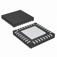
MAX9703ETJ+T Maxim Integrated Products, MAX9703ETJ+T Datasheet - Page 2

MAX9703ETJ+T
Manufacturer Part Number
MAX9703ETJ+T
Description
IC AMP AUDIO PWR 18W MONO 32TQFN
Manufacturer
Maxim Integrated Products
Type
Class Dr
Datasheet
1.MAX9703ETJ.pdf
(20 pages)
Specifications of MAX9703ETJ+T
Output Type
1-Channel (Mono)
Max Output Power X Channels @ Load
18W x 1 @ 16 Ohm
Voltage - Supply
10 V ~ 25 V
Features
Depop, Differential Inputs, Mute, Short-Circuit and Thermal Protection, Shutdown
Mounting Type
Surface Mount
Package / Case
32-TQFN Exposed Pad
Lead Free Status / RoHS Status
Lead free / RoHS Compliant
ABSOLUTE MAXIMUM RATINGS
(All voltages referenced to PGND.)
V
OUTR_, OUTL_, C1N..................................-0.3V to (V
C1P............................................(V
CHOLD ........................................................(V
All Other Pins to PGND...........................................-0.3V to +12V
Duration of OUTR_/OUTL_
Continuous Input Current (V
Continuous Input Current......................................................0.8A
Continuous Input Current (all other pins)..........................±20mA
10W Stereo/15W Mono, Filterless,
Spread-Spectrum, Class D Amplifiers
ELECTRICAL CHARACTERISTICS
(V
= PGND (f
noted. Typical values are at T
Stresses beyond those listed under “Absolute Maximum Ratings” may cause permanent damage to the device. These are stress ratings only, and functional
operation of the device at these or any other conditions beyond those indicated in the operational sections of the specifications is not implied. Exposure to
absolute maximum rating conditions for extended periods may affect device reliability.
2
GENERAL
Supply Voltage Range
Quiescent Current
Shutdown Current
Turn-On Time
Amplifier Output Resistance in
Shutdown
Input Impedance
Voltage Gain
Gain Matching
Output Offset Voltage
Common-Mode Rejection Ratio
Power-Supply Rejection Ratio
(Note 3)
DD
DD
Short Circuit to PGND, V
_______________________________________________________________________________________
to PGND, AGND .............................................................30V
= 15V, AGND = PGND = 0V, SHDN ≥ V
PARAMETER
S
= 660kHz), R
L
DD
DD
connected between OUTL+ and OUTL- and OUTR+ and OUTR-, T
A
................................................10s
, PGND) ...............................1.6A
= +25°C.) (Notes 1, 2)
DD
SYMBOL
CMRR
I
PSRR
- 0.3V) to (CHOLD + 0.3V)
SHDN
V
V
I
t
R
A
DD
ON
DD
OS
IN
V
DD
IH
Inferred from PSRR test
R
C
C
SHDN = PGND
A
A
A
A
G1 = L, G2 = L
G1 = L, G2 = H
G1 = H, G2 = L
G1 = H, G2 = H
Between channels (MAX9704)
f
V
200mV
IN
, A
DD
L
V
V
V
V
SS
SS
- 0.3V) to +40V
= OPEN
= 1kHz, input referred
= 13dB
= 16dB
= 19.1dB
= 29.6dB
V
= 470nF
= 180nF
= 10V to 25V
= 16dB, C
DD
P-P
+ 0.3V)
ripple
SS
CONDITIONS
= C
IN
Continuous Power Dissipation (T
Single-Layer Board:
Multilayer Board:
Junction Temperature ......................................................+150°C
Operating Temperature Range ...........................-40°C to +85°C
Storage Temperature Range .............................-65°C to +150°C
Lead Temperature (soldering, 10s) .................................+300°C
MAX9703
MAX9704
f
f
RIPPLE
RIPPLE
MAX9703 32-Pin TQFN (derate 21.3mW/°C
above +70°C)..........................................................1702.1mW
MAX9704 32-Pin TQFN (derate 27mW/°C
above +70°C)..........................................................2162.2mW
MAX9703 32-Pin TQFN (derate 34.5mW/°C
above +70°C)..........................................................2758.6mW
MAX9704 32-Pin TQFN (derate 37mW/°C
above +70°C)..........................................................2963.0mW
= 0.47µF, C
= 1kHz
= 20kHz
REG
= 0.01µF, C1 = 100nF, C2 = 1µF, FS1 = FS2
A
29.4
18.9
12.8
15.9
MIN
150
10
35
30
23
10
54
= T
A
MIN
= +70°C)
to T
TYP
29.6
19.1
100
330
0.2
0.5
14
24
50
58
48
39
15
13
16
±6
60
80
80
66
MAX
, unless otherwise
MAX
29.8
19.3
13.2
16.3
±30
1.5
25
22
34
80
65
55
22
UNITS
mA
mV
ms
µA
kΩ
kΩ
dB
dB
dB
%
V


