MAX9709ETN+TD Maxim Integrated Products, MAX9709ETN+TD Datasheet - Page 2
MAX9709ETN+TD
Manufacturer Part Number
MAX9709ETN+TD
Description
IC AMP AUDIO PWR 50W STER 56TQFN
Manufacturer
Maxim Integrated Products
Type
Class Dr
Datasheet
1.MAX9709ETND.pdf
(20 pages)
Specifications of MAX9709ETN+TD
Output Type
1-Channel (Mono) or 2-Channel (Stereo)
Max Output Power X Channels @ Load
50W x 1 @ 4 Ohm; 29W x 2 @ 8 Ohm
Voltage - Supply
10 V ~ 22 V
Features
Depop, Differential Inputs, Mute, Short-Circuit and Thermal Protection, Shutdown
Mounting Type
Surface Mount
Package / Case
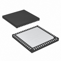
56-TQFN
Lead Free Status / RoHS Status
Lead free / RoHS Compliant


ABSOLUTE MAXIMUM RATINGS
PV
PV
OUTR+, OUTR-, OUTL+,
C1N to GND .............................................-0.3V to (PV
C1P to GND..............................(PV
CPV
All Other Pins to GND.............................................-0.3V to +12V
Continuous Input Current (except PV
25W/50W, Filterless, Spread-Spectrum,
Stereo/Mono, Class D Amplifier
ELECTRICAL CHARACTERISTICS
(PV
mode), SHDN = MUTE = high, G1 = low, G2 = high (A
connected between OUT_+ and OUT_-, unless otherwise stated. T
= +25°C.) (Note 1)
Stresses beyond those listed under “Absolute Maximum Ratings” may cause permanent damage to the device. These are stress ratings only, and functional
operation of the device at these or any other conditions beyond those indicated in the operational sections of the specifications is not implied. Exposure to
absolute maximum rating conditions for extended periods may affect device reliability.
2
Supply Voltage Range
Shutdown Current
Shutdown to Full Operation
Mute to Full Operation
Input Impedance
Output Pulldown Resistance
Output Offset Voltage
Power-Supply Rejection Ratio
Common-Mode Rejection Ratio
Switch On-Resistance
Switching Frequency
Oscillator Spread Bandwidth
SYNCIN Lock Range
OUTL- to PGND, GND..........................-0.3V to (PV
OUTR-, OUTL+, and OUTL-) ..........................................20mA
DD
DD
DD
_______________________________________________________________________________________
DD
, V
to V
= V
to GND ..........................................(PV
DD
DD
DD
PARAMETER
to PGND, GND .......................................-0.3 to +30V
..........................................................-0.3V to +0.3V
= +20V, PGND = GND = 0V, C
DD
DD
SYMBOL
- 0.3V) to (CPV
CMRR
, V
I
t
PSRR
SHDN
t
MUTE
V
V
R
f
SON
R
SW
DD
OS
DS
DD
IN
, OUTR+,
DD
SS
- 0.3V) to +40V
= 0.47µF, C
Inferred from PSRR test
SHDN = low
G1 = 0, G2 = 1
G1 = 1, G2 = 1
G1 = 1, G2 = 0
G1 = 0, G2 = 0
SHDN = GND
AC-coupled input, measured between
OUT_+ and OUT_-
PV
200mV
(Note 2)
DC, input referred
f = 20Hz to 20kHz, input referred
One power switch
FS1
0
1
1
0
FS1 = FS2 = high (SSM)
Equal to f
DD
DD
DD
DD
V
= 10V to 22V
+ 0.3V)
+ 0.3V)
+ 0.3V)
P-P
= 22dB), FS1 = FS2 = high (SSM), SYNCIN = low. All load resistors (R
SW
ripple
REG
x 4
CONDITIONS
= 0.01µF, C1 = 0.1µF, C2 = 1µF, R
A
= T
Continuous Power Dissipation (T
Operating Temperature Range ...........................-40°C to +85°C
Storage Temperature Range .............................-65°C to +150°C
Junction Temperature ......................................................+150°C
Thermal Resistance (θ
Lead Temperature (soldering, 10s) .................................+300°C
FS2
0
1 (SSM)
0
1
f
f
RIPPLE
RIPPLE
56-Pin Thin QFN (derate 47.6mW/°C above +70°C) .....3.81W
56-Pin Thin QFN… ......................................................0.6°C/W
MIN
to T
= 1kHz
= 20kHz
MAX
, unless otherwise noted. Typical values are at T
JC
)
MIN
180
600
50
10
40
25
12
67
49
LOAD
A
= +70°C)
TYP
100
100
600
200
200
160
250
= ∞, MONO = low (stereo
0.1
0.3
±2
85
63
43
21
90
90
52
70
60
3
MAX
1200
±40
125
220
0.6
22
90
60
30
1
UNITS
kHz
kHz
mV
ms
ms
µA
kΩ
kΩ
dB
dB
%
L
Ω
V
) are
A
Related parts for MAX9709ETN+TD
Image
Part Number
Description
Manufacturer
Datasheet
Request
R

Part Number:
Description:
25W/50W Filterless Spread-Spectrum Stereo/Mono Class D Amplifier
Manufacturer:
Maxim Integrated Products
Datasheet:

Part Number:
Description:
Max9709 25w/50w, Filterless, Spread-spectrum, Stereo/mono, Class D Amplifier
Manufacturer:
Maxim Integrated Products, Inc.
Datasheet:
Part Number:
Description:
MAX7528KCWPMaxim Integrated Products [CMOS Dual 8-Bit Buffered Multiplying DACs]
Manufacturer:
Maxim Integrated Products
Datasheet:
Part Number:
Description:
Single +5V, fully integrated, 1.25Gbps laser diode driver.
Manufacturer:
Maxim Integrated Products
Datasheet:
Part Number:
Description:
Single +5V, fully integrated, 155Mbps laser diode driver.
Manufacturer:
Maxim Integrated Products
Datasheet:
Part Number:
Description:
VRD11/VRD10, K8 Rev F 2/3/4-Phase PWM Controllers with Integrated Dual MOSFET Drivers
Manufacturer:
Maxim Integrated Products
Datasheet:
Part Number:
Description:
Highly Integrated Level 2 SMBus Battery Chargers
Manufacturer:
Maxim Integrated Products
Datasheet:
Part Number:
Description:
Current Monitor and Accumulator with Integrated Sense Resistor; ; Temperature Range: -40°C to +85°C
Manufacturer:
Maxim Integrated Products
Part Number:
Description:
TSSOP 14/A°/RS-485 Transceivers with Integrated 100O/120O Termination Resis
Manufacturer:
Maxim Integrated Products
Part Number:
Description:
TSSOP 14/A°/RS-485 Transceivers with Integrated 100O/120O Termination Resis
Manufacturer:
Maxim Integrated Products
Part Number:
Description:
QFN 16/A°/AC-DC and DC-DC Peak-Current-Mode Converters with Integrated Step
Manufacturer:
Maxim Integrated Products
Part Number:
Description:
TDFN/A/65V, 1A, 600KHZ, SYNCHRONOUS STEP-DOWN REGULATOR WITH INTEGRATED SWI
Manufacturer:
Maxim Integrated Products
Part Number:
Description:
Integrated Temperature Controller f
Manufacturer:
Maxim Integrated Products
Part Number:
Description:
SOT23-6/I°/45MHz to 650MHz, Integrated IF VCOs with Differential Output
Manufacturer:
Maxim Integrated Products
Part Number:
Description:
SOT23-6/I°/45MHz to 650MHz, Integrated IF VCOs with Differential Output
Manufacturer:
Maxim Integrated Products