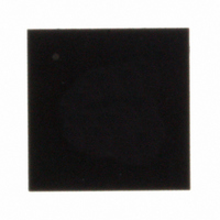
LX1725ILQ Microsemi Analog Mixed Signal Group, LX1725ILQ Datasheet - Page 20

LX1725ILQ
Manufacturer Part Number
LX1725ILQ
Description
IC AMP AUDIO 32W STER D 32MLPQ
Manufacturer
Microsemi Analog Mixed Signal Group
Series
AudioMAX™r
Type
Class Dr
Datasheet
1.LX1725ILQ.pdf
(23 pages)
Specifications of LX1725ILQ
Output Type
1-Channel (Mono) or 2-Channel (Stereo)
Max Output Power X Channels @ Load
32W x 1 @ 8 Ohm; 16W x 2 @ 4 Ohm
Voltage - Supply
12 V ~ 35 V, ±6 V ~ 17.5 V
Features
Depop, Differential Inputs, Mute, PWM, Short-Circuit and Thermal Protection, Standby
Mounting Type
Surface Mount
Package / Case
32-MLPQ
Lead Free Status / RoHS Status
Lead free / RoHS Compliant
Copyright © 2004
Rev. 1.2, 2005-12-06
PCB D
One of the key efforts in implementing the MLP package
on a pc board is the design of the land pattern. The MLP
has rectangular metallized terminals exposed on the bottom
surface of the package body. Electrical and mechanical
connection between the component and the pc board is
made by screen printing solder paste on the pc board and
then reflowing the paste after placement. To guarantee
reliable solder joints it is essential to design the land pattern
to the MLP terminal pattern, exposed PAD, and Thermal
PAD via. There are two basic designs for PCB land pads
for the MLP: Copper Defined style (also known as Non
Solder Mask Defined (NSMD)) and the Solder Mask
Defined style (SMD). The industry has had some debate on
the merits of both styles and although Microsemi
recommends the Copper Defined style land pad (NSMD),
both styles are acceptable for use with the MLP package.
NSMD pads are recommended over SMD pads due to the
tighter tolerance on copper etching than solder masking.
NSDM by definition also provides a larger copper pad area
and allows the solder to anchor to the edges of the copper
pads thus providing improved solder joint reliability.
D
T
As a general rule, the PCB lead finger pad (Y) should be
designed 0.2-0.5mm longer than the package terminal
length for good filleting. The pad length should extend
0.05mm towards the centerline of the package. The pad
width (X) should be a minimum 0.05mm wider than the
package terminal width (0.025mm per side), refer to figure
21. However, the pad width is reduced to the width of the
component terminal for lead pitches below 0.65mm. This is
done to minimize the risk of solder bridging.
Figure 21 – PC Board Land Pattern Geometry for MLP Terminals
ERMINALS
ESIGN
TM
ESIGN
0.05mm
Y2
OF
G
PCB L
UIDELINES
11861 Western Avenue, Garden Grove, CA. 92841, 714-898-8121, Fax: 714-893-2570
AND
0.20mm
Part
Part Lead
Solder
PCB Pad
PCB
Y1
P
ATTERN
P C B D E S I G N G U I D E L I N E S
FOR
Integrated Products Division
P
(X1) Min: 0.025mm
Per side for lead
pitches > 0.65mm
®
ACKAGE
Microsemi
E
The construction of the Exposed Pad MLP enables
enhanced thermal and electrical characteristics. In order to
take full advantage of this feature the exposed pad must be
physically connected to the PCB substrate with solder. The
exposed pad is internally connected to the die substrate
potential which is VNEG so it is very important that the
PCB substrate potential be connected to VNEG as well.
The thermal pad (D2th) should be greater than D2 of the
MLP whenever possible; however adequate clearance (Cpl
> 0.15mm) must be met to prevent solder bridging. If this
clearance cannot be met, then D2th should be reduced in
area. The formula would be: D2TH >D2 only if D2TH <
Gmin - (2 x Cpl).
T
There are two types of on-board thermal PAD designs: one
is using thermal vias to sink the heat to the other layer with
metal traces. Based on the Jedec Specification (JESD 51-5)
the thermal vias should be designed like Figure 22.
Another one is the no via thermal PAD which is using the
same side copper PAD as heat sink, this type of thermal
PAD is good for a two layer board, since the bottom side is
filled with all other kinds of trace also, it’s hard to use the
whole plane for the heat sink. But you still can use vias to
sink the heat to the bottom layer by the metal traces, then
layout a NMSD on which a metal heat sink is put to sink
the heat to the air.
XPOSED
HERMAL
Package Land Pattern
Micro Lead Quad
15W+15W Stereo Class-D Amplifier
Figure 22 – Comparison of land pattern theory
P
Filterless 30W Mono in BTL
P
AD
AD
P
PCB D
RODUCTION
V
IA
D
ESIGN
ESIGN
D
ATA
Layer Board with Vias
Land Pattern for Four
S
HEET
LX1725
Page
20


