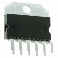
TDA7391 STMicroelectronics, TDA7391 Datasheet

TDA7391
Specifications of TDA7391
Available stocks
Related parts for TDA7391
TDA7391 Summary of contents
Page 1
... This is advanced information on a new product now in development or undergoing evaluation. Details are subject to change without notice. 35W BRIDGE CAR RADIO AMPLIFIER ORDERING NUMBER: TDA7391 ESD DESCRIPTION The TDA7391 is a BRIDGE class AB audio power amplifier specially intended for car radio High Power applications. The high power capability together with the possi- bility to operate either in DIFFERENTIAL INPUT ...
Page 2
... TDA7391 Figure 2: Block Diagram V V CC1 CC2 STANDBY THRESHOLD 1 IN- ICM 2 IN+ PROGRAMMABLE + CURRENT CIRCUIT - MUTE THRESHOLD 11 MUTE PIN CONNECTION (Top view) TAB CONNECTED TO PIN 6 THERMAL DATA Symbol R Thermal Resistance Junction-case th j-case 2/8 REFERENCES POWER AMP COMMON MODE - LTS + V CC/2 - POWER AMP ...
Page 3
... Saturated sqare wave output. Parameter = 14.4V 1KHz Test Condition V = 1.5V ST- ST- 5V) MUTE 13.7V 3 14.4V 3 0.1 to 15W 1W; -3dB O Differential Single Ended 22Hz to 22KHz 1KHz 1Vrms 1Vrms g r TDA7391 Value Unit 4 -40 to 150 unless otherwise amb Min. Typ. Max. Unit 150 mA 120 mV 100 1 ...
Page 4
... Supply Voltage. S The TDA7391 is equipped with a diagnostic circuitry able to detect the clipping in the 4 CD Output Signal (distortion = 10%). The CD pin (open collector) gives out low level signal during clipping. The output stage is a bridge type able to drive loads as low as 3.2 . ...
Page 5
... Figure 4: Quiescent Current vs Supply Voltage Figure 6: Output Power vs Supply Voltage (@ 1KHz Figure 8: Output Power vs Supply Voltage (@ 1KHz Figure 5: EIAJ power vs Supply Voltage Figure 7: Distortion vs Frequency (@ (Hz) Figure 9: Distortion vs Frequency ( (Hz) TDA7391 = 14. 12W 14. 3 15W O 5/8 ...
Page 6
... TDA7391 Figure 10: Supply Voltage Rejection vs Fre- quency f = (Hz) Figure 12: TotalPower Dissipation & Efficiency vs. Output Power (@ (W) O 6/8 Figure 11: Common Mode Rejection vs. Fre- quency V = 14. 1Vrms Figure 13: Power Bandwidth V = 14. 14. 1KHz 14. 1Vrms (Hz (Hz) ...
Page 7
... S 1.9 2.6 0.075 S1 1.9 2.6 0.075 Dia1 3.65 3.85 0.144 OUTLINE AND MAX. MECHANICAL DATA 0.197 0.104 0.063 0.022 0.037 0.077 0.679 0.795 0.886 0.886 0.713 0.699 0.429 0.114 0.191 0.214 0.102 Multiwatt11 V 0.102 0.152 TDA7391 7/8 ...
Page 8
... TDA7391 Information furnished is believed to be accurate and reliable. However, STMicroelectronics assumes no responsibility for the consequences of use of such information nor for any infringement of patents or other rights of third parties which may result from its use. No license is granted by implication or otherwise under any patent or patent rights of STMicroelectronics. Specification mentioned in this publication are subject to change without notice ...


