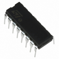
TDA1904 STMicroelectronics, TDA1904 Datasheet

TDA1904
Specifications of TDA1904
Available stocks
Related parts for TDA1904
TDA1904 Summary of contents
Page 1
... Peak output current (repetitive Total power dissipation at T tot Storage and junction temperature stg j TEST AND APPLICATION CIRCUIT (*) R4 is necessary only for V September 2003 ORDERING NUMBER : TDA 1904 Parameter = 80 C amb pins < 6V. s TDA1904 4W AUDIO AMPLIFIER Powerdip ( Value 20 2 -40 to 150 Unit 1/10 ...
Page 2
... TDA1904 PIN CONNECTION BOOTSTRAP NON INVERT. IN SCHEMATIC DIAGRAM THERMAL DATA Symbol R Thermal resistance junction-pins th-j-case R Thermal resistance junction-ambient th-j-amb 2/10 OUTPUT N.C. 4 N.C. 5 INVERT SVR 7 8 D95AU319 Parameter 16 GND 15 GND 14 GND 13 GND 12 GND 11 GND 10 GND 9 GND Value max 15 max 70 Unit C/W ...
Page 3
... KHz 1. 14V KHz KHz 14V 4. 14V 14V KHz V = 14V KHz 12V 100 ripple 0.5 Vrms ripple tot TDA1904 (heatsink Min. Typ. Max. Unit 2 4.5 W 3.1 0.7 0.1 0.3 % 0.8 V 1.3 55 150 40,000 39.5 40 40 120 ÉC 3/10 ...
Page 4
... TDA1904 Figure 1. Test and application circuit (*) R4 is necessary only for V Figure 2. P.C. board and components layout of fig scale) 4/10 < ...
Page 5
... Increase of gain. Decrease of gain. Danger of oscillation at high frequencies with inductive loads. Higher cost lower noise. Increase of SVR increase of the switch-on time. Increase of the switch-on noise TDA1904 Allowed range Smaller than recommended value Min. Decrease of gain. 9R3 Increase quiescent current. Increase of gain. 39 220 Higher low frequency cutoff ...
Page 6
... TDA1904 Figure 3. Quiescent output voltage vs. supply voltage Fi gure 6. Distor tion vs. output power Fi gure 9. Distor tion vs. output power 6/10 Figure 4. Quiescent drain current vs. supply voltage Fi gure 7. Distor tion vs. output power Figure 10. Distortion vs. output power Figure 5. Output power vs. supply voltage Fig ure 8. Distortion vs. ...
Page 7
... Figure 13. Distortion vs. frequency Figure 16. Supply voltage rejection vs. frequency 19. Total p ower dissipation and efficiency vs. output power TDA1904 Figure 14. Distortion vs. frequency Fi g ure 1 7. Total power dissipation and efficiency vs. output power Fi g ure 2 0. Total power dissipation and efficiency vs. output power ...
Page 8
... TDA1904 THERMAL SHUT-DOWN The presence of a thermal limiting circuit offers the following advantages overload on the output (even perma- nent above limit ambient temperature can be easily tolerated since the T higher than 150 C. 2) The heatsink can have a smaller factor of safety compared with that of a conventional circuit. ...
Page 9
... TYP. MAX. MIN. a1 0.51 0.020 B 0.85 1.40 0.033 b 0.50 b1 0.38 0.50 0.015 D 20.0 E 8.80 e 2.54 e3 17.78 F 7.10 I 5.10 L 3.30 Z 1.27 inch MECHANICAL DATA TYP. MAX. 0.055 0.020 0.020 0.787 0.346 0.100 0.700 0.280 0.201 0.130 0.050 TDA1904 OUTLINE AND Powerdip 16 9/10 ...
Page 10
... TDA1904 Information furnished is believed to be accurate and reliable. However, STMicroelectronics assumes no responsibility for the consequences of use of such information nor for any infringement of patents or other rights of third parties which may result from its use. No license is granted by implication or otherwise under any patent or patent rights of STMicroelectronics. Specifications mentioned in this publication are subject to change without notice ...


