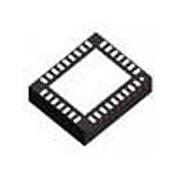
LM4918LQ/NOPB National Semiconductor, LM4918LQ/NOPB Datasheet - Page 11

LM4918LQ/NOPB
Manufacturer Part Number
LM4918LQ/NOPB
Description
IC AMP AUDIO PWR 1.1W STER 32LLP
Manufacturer
National Semiconductor
Series
Boomer®r
Type
Class ABr
Datasheet
1.LM4918LQNOPB.pdf
(17 pages)
Specifications of LM4918LQ/NOPB
Output Type
2-Channel (Stereo)
Max Output Power X Channels @ Load
1.1W x 2 @ 8 Ohm
Voltage - Supply
2.7 V ~ 5.5 V
Features
Depop, Mute, Shutdown, Thermal Protection, Volume Control
Mounting Type
Surface Mount
Package / Case
32-LLP
Operational Class
Class-AB
Audio Amplifier Output Configuration
2-Channel Stereo
Output Power (typ)
1.1x2@8OhmW
Audio Amplifier Function
Speaker
Total Harmonic Distortion
0.3@8Ohm@1W%
Single Supply Voltage (typ)
3/5V
Dual Supply Voltage (typ)
Not RequiredV
Power Supply Requirement
Single
Rail/rail I/o Type
No
Power Supply Rejection Ratio
67dB
Single Supply Voltage (min)
2.7V
Single Supply Voltage (max)
5.5V
Dual Supply Voltage (min)
Not RequiredV
Dual Supply Voltage (max)
Not RequiredV
Operating Temp Range
-40C to 85C
Operating Temperature Classification
Industrial
Mounting
Surface Mount
Pin Count
32
Package Type
LLP EP
Lead Free Status / RoHS Status
Lead free / RoHS Compliant
Other names
LM4918LQ
Application Information
mize thermal design may compromise the LM4918’s perfor-
mance and activate unwanted, though necessary, thermal
shutdown protection.
The LM4918LD must have its DAP soldered to a copper pad
on the PCB. The DAP’s PCB copper pad is then, ideally,
connected to a large plane of continuous unbroken copper.
This plane forms a thermal mass, heat sink, and radiation
area. Place the heat sink area on either outside plane in the
case of a two-sided or multi-layer PCB. (The heat sink area
can also be placed on an inner layer of a multi-layer board.
The thermal resistance, however, will be higher.) Connect
the DAP copper pad to the inner layer or backside copper
heat sink area with 2 vias. The via diameter should be
0.012in - 0.013in with a 1.27mm pitch. Ensure efficient ther-
mal conductivity by plugging and tenting the vias with plating
and solder mask, respectively. Further detailed and specific
information concerning PCB layout, fabrication, and mount-
ing an LQ (LLP) package is available in National Semicon-
ductor’s AN1187.
FIGURE 2. REFERENCE DESIGN BOARD SCHEMATIC
(Continued)
11
POWER SUPPLY BYPASSING
As with any power amplifier, proper supply bypassing is
critical for low noise performance and high power supply
rejection. Applications that employ a 5V regulator typically
use a 10µF in parallel with a 0.1µF filter capacitors to stabi-
lize the regulator’s output, reduce noise on the supply line,
and improve the supply’s transient response. However, their
presence does not eliminate the need for a local 1.0µF
tantalum bypass capacitance connected between the
LM4918’s supply pins and ground. Keep the length of leads
and traces that connect capacitors between the LM4918’s
power supply pin and ground as short as possible. Connect-
ing a 2.2µF capacitor, C
ground improves the internal bias voltage’s stability and
improves the amplifier’s PSRR. The PSRR improvements
increase as the bypass pin capacitor value increases. Too
large, however, increases turn-on time and can compromise
the amplifier’s click and pop performance. The selection of
bypass capacitor values, especially C
PSRR requirements, click and pop performance system
cost, and size constraints.
B
, between the BYPASS pin and
B
, depends on desired
www.national.com
200913I8


