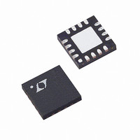
LTC6401IUD-26#PBF Linear Technology, LTC6401IUD-26#PBF Datasheet - Page 12

LTC6401IUD-26#PBF
Manufacturer Part Number
LTC6401IUD-26#PBF
Description
IC ADC DRIVER DIFF 16-QFN
Manufacturer
Linear Technology
Type
ADC Driverr
Datasheet
1.LTC6401CUD-26PBF.pdf
(16 pages)
Specifications of LTC6401IUD-26#PBF
Applications
Data Acquisition
Mounting Type
Surface Mount
Package / Case
16-WQFN Exposed Pad
No. Of Amplifiers
1
Input Offset Voltage
2.5mV
Gain Db Max
26dB
Bandwidth
1.6GHz
Slew Rate
3300V/µs
Supply Voltage Range
2.85V To 3.5V
Supply Current
45mA
Amplifier Case Style
QFN
Rohs Compliant
Yes
Lead Free Status / RoHS Status
Lead free / RoHS Compliant
Available stocks
Company
Part Number
Manufacturer
Quantity
Price
APPLICATIONS INFORMATION
LTC6401-26
of the LTC6401-26 is connected to V
at 1.25V. Alternatively, a single-ended input signal can be
converted to a differential signal via a balun and fed to the
input of the LTC6401-26. Figure 8 summarizes the IMD3
performance of the whole system as shown in Figure 7.
Test Circuits
Due to the fully-differential design of the LTC6401 and
its usefulness in applications with differing characteristic
specifi cations, two test circuits are used to generate the
information in this datasheet. Test Circuit A is DC987B,
a two-port demonstration circuit for the LTC6401 family.
The silkscreen is shown in Figure 9. This circuit includes
input and output transformers (baluns) for single-ended-
to-differential conversion and impedance transformation,
allowing direct hook-up to a 2-port network analyzer.
There are also series resistors at the output to present the
LTC6401 with a 375Ω differential load, optimizing distortion
performance. Due to the input and output transformers, the
–3dB bandwidth is reduced from 1.6GHz to 1.37GHz.
12
13
14
15
16
Figure 6. LTC6401-26 with 165MHz Output Bandpass Filter
Figure 7. Single-Ended Input to LTC6401-26 and LTC2208
IF IN
+IN
+IN
–IN
–IN
150Ω
25Ω
25Ω
37.4Ω
IN+
IN–
0.1μF
0.1μF
500Ω
500Ω
OUT–
OUT+
+IN
–IN
ENABLE
LTC6401-26
V
OCM
+OUT
–OUT
12.5Ω
12.5Ω
50Ω
50Ω
+OUTF
–OUTF
26dB GAIN
LTC6401-26
1.7pF
+OUTF
–OUTF
0.1μF
+OUT
–OUT
640126 F06
4.99Ω
4.99Ω
8
7
6
5
10Ω
10Ω
1.25V
16nH
39pF
39pF
CM
of the LTC2208
AIN
AIN
4.99Ω
4.99Ω
LTC2208 130Msps
39pF
–
+
LTC2208
16-Bit ADC
V
CM
640126 F07
LTC2208
Test Circuit B uses a 4-port network analyzer to measure
S-parameters and gain/phase response. This removes the
effects of the wideband baluns and associated circuitry,
for a true picture of the >1GHz S-parameters and AC
characteristics.
Figure 8. IMD
Figure 9. Top Silkscreen for DC987B, Test Circuit A
3
–100
–110
–40
–50
–60
–70
–80
–90
for the Combination of LTC6401-26 and LTC2208
0
SINGLE-ENDED INPUT
F
DRIVER V
S
= 122.8Msps
50
OUT
FREQUENCY (MHz)
= 2V
P-P
100
COMPOSITE
150
640126 F08
200
640126f


