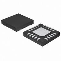
MAX3272AETP+ Maxim Integrated Products, MAX3272AETP+ Datasheet - Page 8

MAX3272AETP+
Manufacturer Part Number
MAX3272AETP+
Description
IC AMP LIMITING 20-TQFN
Manufacturer
Maxim Integrated Products
Type
Limiting Amplifierr
Datasheet
1.MAX3272AETP.pdf
(14 pages)
Specifications of MAX3272AETP+
Applications
Optical Networks
Mounting Type
Surface Mount
Package / Case
20-TQFN Exposed Pad
Input Voltage Range (max)
1200 mV
Operating Supply Voltage
3.3 V
Supply Current
33 mA
Operating Temperature Range
- 40 C to + 85 C
Mounting Style
SMD/SMT
Power Dissipation
1100 mW
Amplifier Type
Low Power
Supply Voltage Range
3V To 3.6V
Amplifier Case Style
TQFN
No. Of Pins
20
Termination Type
SMD
Supply Voltage Min
3V
Rohs Compliant
Yes
Filter Terminals
SMD
Lead Free Status / RoHS Status
Lead free / RoHS Compliant
The MAX3272/MAX3272A CML output circuit (Figure 5)
provides high tolerance to impedance mismatches and
inductive connectors. The output current can be set to
two levels using the LEVEL pin. When LEVEL is uncon-
nected, the output current is approximately 16mA.
Connecting LEVEL to ground sets the output current to
approximately 20mA. The squelch function is enabled
when the SQUELCH pin is set to a TTL high. This func-
tion holds OUT+ and OUT- to a static level whenever
the input signal amplitude drops below the loss-of-sig-
nal threshold. This circuit is also equipped with a polari-
ty selector, programmed by the OUTPOL pin. When
this pin is connected to V
When connected to ground, the output signal will be
inverted.
+3.3V, 2.5Gbps Low-Power
Limiting Amplifiers
8
Figure 5. CML Output Circuit
_______________________________________________________________________________________
50Ω
GND
V
CC
LEVEL
50Ω
CC
, no inversion will occur.
CML Output Buffer
OUT+
OUT-
ESD
STRUCTURES
External resistor R
threshold. See the LOS Threshold vs. R
the Typical Operating Characteristics section to select
the appropriate resistor.
When AC-coupling, input and output coupling capaci-
tors (C
receiver’s deterministic jitter. Jitter is decreased as the
input low-frequency cutoff (f
For ATM/SONET or other applications using scrambled
NRZ data, select (C
f
other applications using 8B/10B data coding, select
(C
Refer to application note HFAN-1.1: Choosing AC-
Coupling Capacitors.
The capacitor between CAZ1 and CAZ2 determines the
time constant of the signal path DC offset-cancellation
loop. To maintain stability, it is important to keep a one-
decade separation between f
cutoff (f
circuit. For ATM/SONET or other applications using
scrambled NRZ data, f
3.2kHz. Therefore, C
Channel or Gigabit Ethernet applications, leave pins
CAZ1 and CAZ2 open.
External capacitor C
and deassert times. When inputting data with many
consecutive identical digits (CIDs), a longer time con-
stant may be advantageous, so LOS does not flag
incorrectly. In this case, connect the CLOS pin to a
0.01µF capacitor to set the assert time in the range of
2µs to 100µs. For scrambled data where the mark den-
sity is kept at 50%, a shorter time constant may be
desirable. Leave the CLOS pin open for a shorter time
constant of about 1µs.
IN
IN
< 32kHz. For Fibre Channel, Gigabit Ethernet, or
, C
IN
OUT
OC
and C
Program the LOS Assert Threshold
) associated with the DC offset-cancellation
) ≥ 0.01µF, which provides f
Program the LOS Time Constant
Select the Coupling Capacitors
OUT
f
IN
Select the Offset-Correction
) should be selected to minimize the
= 1 / [2π(50)(C
IN
AZ
TH
CLOS
, C
= 0.1µF (f
programs the loss-of-signal
OUT
IN
Design Procedure
IN
programs the LOS assert
) ≥ 0.1µF, which provides
< 32kHz, so f
) is decreased:
IN
and the low-frequency
OC
IN
)]
= 2kHz). For Fibre
TH
IN
Capacitor
graph in the
< 320kHz.
OCMAX
<


