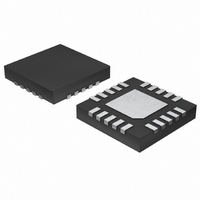
MAX3964AETP+ Maxim Integrated Products, MAX3964AETP+ Datasheet - Page 2

MAX3964AETP+
Manufacturer Part Number
MAX3964AETP+
Description
IC AMP LIMITING SGNL DET 20-TQFN
Manufacturer
Maxim Integrated Products
Type
Limiting Amplifierr
Datasheet
1.MAX3964AETP.pdf
(11 pages)
Specifications of MAX3964AETP+
Applications
Optical Networks
Mounting Type
Surface Mount
Package / Case
20-TQFN Exposed Pad
Operating Supply Voltage
5 V
Supply Current
22 mA
Operating Temperature Range
+ 85 C
Mounting Style
SMD/SMT
Number Of Channels
1
Power Dissipation
1349 mW
Lead Free Status / RoHS Status
Lead free / RoHS Compliant
ABSOLUTE MAXIMUM RATINGS
(SUB, GND tied to ground)
V
FILTER, RSSI, IN+, IN-, CZP, CZN, SQUELCH,
PECL Output Current (OUT+, OUT-, LOS+, LOS-) ............50mA
Differential Voltage Between CZP and CZN..........-1.5V to +1.5V
Differential Voltage Between IN+ and IN- .............-1.5V to +1.5V
+3.0V to +5.5V, 125Mbps to 266Mbps
Limiting Amplifiers with Loss-of-Signal Detector
Stresses beyond those listed under “Absolute Maximum Ratings” may cause permanent damage to the device. These are stress ratings only, and functional
operation of the device at these or any other conditions beyond those indicated in the operational sections of the specifications is not implied. Exposure to
absolute maximum rating conditions for extended periods may affect device reliability.
ELECTRICAL CHARACTERISTICS—MAX3964ACEP/MAX3968CEP
(V
are at V
2
Supply Current
LOS Hysteresis
SQUELCH Input Current
PECL Output Voltage High
PECL Output Voltage Low
PECL LOS Output Voltage High
PECL LOS Output Voltage Low
LOS Assert Accuracy
Minimum LOS Assert Input
Maximum LOS Deassert Input
Input Sensitivity
Input Overload
Output Transition Time
Pulse-Width Distortion
CC
LOS+, LOS-, INV, VTH, OUT+, OUT- ......-0.5V to (V
CC
, V
_______________________________________________________________________________________
= +3.0V to +5.5V, PECL outputs terminated with 50Ω to (V
CCO
CC
.............................................................-0.5V to +7.0V
PARAMETER
= +3.3V and T
A
= +25°C.) (Note 1)
SYMBOL
I
t
CC
r
, t
f
PECL outputs open
Input = 3.3mV
V
(Note 3)
(Note 3)
(Note 3)
(Note 3)
Input = 7mV
20% to 80% transition time, MAX3964A
MAX3968
(Note 4)
SQUELCH
CC
+ 0.5V)
= V
P-P
P-P
CC
CC
CONDITIONS
or 90mV
, T
to 90mV
- 2V), T
Continuous Power Dissipation (T
Operating Temperature Range ...........................-40°C to +85°C
Operating Junction Temperature Range (die) .....-40°C to +150°C
Processing Temperature (die) ........................................+400°C
Storage Temperature Range .......................... -65°C to +160°C
Lead Temperature (soldering, 10s) ................................+300°C
A
= +25°C
20-Lead Thin QFN
20-Pin QSOP (derate 6.7mW/°C above +70°C)...........500mW
P-P
(derate 16.9mW/°C above +70°C) ..........................1349mW
A
P-P
= 0°C to +70°C, unless otherwise noted. Typical values
(Note 2)
-1025
-1810
-1035
-1810
0.92
MIN
-2.5
143
3.8
1.5
0.4
A
= +70°C)
TYP
2.0
1.2
0.8
22
27
50
5
-1620
-1620
MAX
-880
-880
+2.5
2.20
100
200
8.0
2.7
3.3
1.2
40
UNITS
mV
mV
mV
V
mA
mV
mV
mV
mV
dB
dB
µA
ps
ns
P-P
P-P
P-P
P-P


