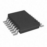
TC1043CEQR Microchip Technology, TC1043CEQR Datasheet - Page 6

TC1043CEQR
Manufacturer Part Number
TC1043CEQR
Description
IC DUAL OPAMP/COMP W/VREF 16QSOP
Manufacturer
Microchip Technology
Type
Amplifier, Comparator, Referencer
Datasheet
1.TC1043CEQR.pdf
(20 pages)
Specifications of TC1043CEQR
Package / Case
16-QSOP
Applications
General Purpose
Mounting Type
Surface Mount
Number Of Channels
2 Channels
Output Type
Push-Pull
Response Time
4 us
Offset Voltage (max)
1.5 mV
Input Bias Current (max)
100 pA
Supply Voltage (max)
5.5 V
Supply Voltage (min)
1.8 V
Supply Current (max)
30 uA
Maximum Operating Temperature
+ 85 C
Mounting Style
SMD/SMT
Minimum Operating Temperature
- 40 C
Lead Free Status / RoHS Status
Lead free / RoHS Compliant
Available stocks
Company
Part Number
Manufacturer
Quantity
Price
Company:
Part Number:
TC1043CEQRTR
Manufacturer:
MICROCHIP
Quantity:
12 000
Part Number:
TC1043CEQRTR
Manufacturer:
MICROCHIP/微芯
Quantity:
20 000
TC1043
4.0
The TC1043 lends itself to a wide variety of applica-
tions, particularly in battery powered systems. It typi-
cally
processor supervisory, and interface circuitry.
4.1
Many microcontrollers have a low power “sleep” mode
that significantly reduces their supply current. Typically,
the microcontroller is placed in this mode via a software
instruction, and returns to a fully enabled state upon
reception of an external signal (“wake-up”). The wake-
up signal is usually supplied by a hardware timer. Most
system applications demand that this timer have a long
duration (typically seconds or minutes), and consume
as little supply current as possible.
The circuit shown in Figure 4-1 is a wake-up timer
made from comparator CMPTR2. (CMPTR2 is used
because the wake-up timer must operate when SHDN
is active.) Capacitor C1 charges through R1 until a volt-
age equal to V
UP is driven active. Upon wake-up, the microcontroller
resets the timer by forcing a logic low on a dedicated,
open drain I/O port pin. This discharges C1 through R4
(the value of R4 is chosen to limit the maximum current
sunk by the I/O port pin). With a 3V supply, the circuit
as shown consumes typically 6µA and furnishes a
nominal timer duration of 25 seconds.
4.2
Figure 4-2 is a precision battery low/battery dead mon-
itoring circuit. Typically, the battery low output warns
the user that a battery dead condition is imminent. Bat-
tery dead typically initiates a forced shutdown to pre-
vent operation at low internal supply voltages (which
can cause unstable system operation).
The circuit of Figure 4-2 uses a single TC1043 (one op
amp is unused) and only six external resistors. AMP 1
is a simple buffer, while CMPTR1 and CMPTR2 provide
precision voltage detection using V
Resistors R2 and R4 set the detection threshold for
BATTLOW, while resistors R1 and R3 set the detection
threshold for BATTFAIL. The component values shown
assert BATTLOW at 2.2V (typical) and BATTFAIL at
2.0V (typical). Total current consumed by this circuit is
typically 22µA at 3V. Resistors R5 and R6 provide hys-
teresis for comparators CMPTR1 and CMPTR2
respectively.
DS21347B-page 6
finds
TYPICAL APPLICATIONS
Wake-Up Timer
Precision Battery Monitor
application
R
is reached, at which point the WAKE-
in
power
R
as a reference.
management,
4.3
Figure 4-3 shows a portion of a TC1043 configured as
a dual low dropout regulator with shutdown. AMP1 and
AMP2 are independent error amplifiers that use V
a reference. Resistors RA
feedback around the amplifiers and therefore deter-
mine the output voltage settings (please see equation
in the figure). RA
ohmic values (i.e. 100’s of kΩ) to minimize supply cur-
rent.
Using the 2N2222 output transistors as shown, these
regulators exhibit low dropout operation. For example,
with V
50mV at an output current of 50mA. The unused com-
parators can be used in conjunction with this circuit as
power-on reset or low voltage detectors for a complete
LDO solution at a very low installed cost.
4.4
Hysteresis can be set externally with two resistors
using positive feedback techniques (see Figure 4-3).
The design procedure for setting external comparator
hysteresis is as follows:
1.
FIGURE 4-1:
2.
3.
10µF
C1
TC1043
Choose the feedback resistor R
input bias current of the comparator is at most
100pA, the current through R
100nA (i.e. 1000 times the input bias current)
and retain excellent accuracy. The current
through R
R
Determine the hysteresis voltage (V
the upper and lower thresholds.
Calculate R
C
OUT
where V
5M
R1
Dual LDO with Shutdown
External Hysteresis
= 3.0V, the typical dropout voltage is only
V
R
C
A
R
at the comparator’s trip point is V
1
R4
as follows:
, RB
is a stable reference voltage.
V
DD
+
–
1
WAKE-UP TIMER
V
, RA
©
DD
CMPTR2
1
2002 Microchip Technology Inc.
, RB
2
and RB
1
, RA
C
I/O*
WAKE-UP
2
*Open Drain Port Pin
2
can be set to
and RB
C
Microcontroller
can have large
HY
. Since the
) between
2
set the
R
R
/
as


