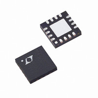
LTC6401IUD-8#PBF Linear Technology, LTC6401IUD-8#PBF Datasheet - Page 5

LTC6401IUD-8#PBF
Manufacturer Part Number
LTC6401IUD-8#PBF
Description
IC ADC DRIVER DIFF 16-QFN
Manufacturer
Linear Technology
Type
ADC Driverr
Datasheet
1.LTC6401CUD-8PBF.pdf
(16 pages)
Specifications of LTC6401IUD-8#PBF
Applications
Data Acquisition
Mounting Type
Surface Mount
Package / Case
16-WQFN Exposed Pad
Lead Free Status / RoHS Status
Lead free / RoHS Compliant
Available stocks
Company
Part Number
Manufacturer
Quantity
Price
AC ELECTRICAL CHARACTERISTICS
⎯ E ⎯ N ⎯ A ⎯ B ⎯ L ⎯ E = 0V, No R
SYMBOL
140MHz Input Signal
HD2,140M/
HD3,140M
IMD3,140M
OIP3,140M
P1dB,140M
NF140M
e
e
IMD3,130M/150M
Note 1: Stresses beyond those listed under Absolute Maximum Ratings
may cause permanent damage to the device. Exposure to any Absolute
Maximum Rating condition for extended periods may affect device
reliability and lifetime.
Note 2: Input pins (+IN, –IN) are protected by steering diodes to either
supply. If the inputs go beyond either supply rail, the input current should
be limited to less than 10mA.
Note 3: The LTC6401C and LTC6401I are guaranteed functional over the
operating temperature range of –40°C to 85°C.
Note 4: The LTC6401C is guaranteed to meet specifi ed performance from
0°C to 70°C. It is designed, characterized and expected to meet specifi ed
TYPICAL PERFORMANCE CHARACTERISTICS
IN,140M
ON,140M
14
12
10
–2
–4
–6
8
6
4
2
0
10
Frequency Response
FREQUENCY (MHz)
100
PARAMETER
Second/Third Order Harmonic Distortion V
Third-Order Intermodulation
(f1 = 139.5MHz f2 = 140.5MHz)
Equivalent Third-Order Output Intercept
Point (f1 = 139.5MHz f2 = 140.5MHz)
1dB Compression Point
Noise Figure
Input Referred Voltage Noise Density
Output Referred Voltage Noise Density
Third-Order Intermodulation
(f1 = 130MHz f2 = 150MHz) Measure at
170MHz
L
unless otherwise noted.
TEST CIRCUIT B
1000
64018 G01
3000
–0.2
–0.4
–0.6
–0.8
–1.0
1.0
0.8
0.6
0.4
0.2
0
10
Gain 0.1dB Flatness
TEST CIRCUIT B
CONDITIONS
V
V
V
V
R
R
Includes Resistors (Short Inputs)
Includes Resistors (Short Inputs)
V
OUT
OUT
OUT
OUT
OUT
L
L
OUT
= 375Ω (Notes 5, 7)
= 375Ω (Note 5)
FREQUENCY (MHz)
= 2V
= 2V
= 2V
= 2V
= 2V
= 2V
100
P-P
P-P
P-P
P-P
P-P
P-P
Specifi cations are at T
, R
, No R
Composite, R
Composite, No R
Composite, No R
Composite, R
L
performance from –40°C to 85°C but is not tested or QA sampled at these
temperatures. The LTC6401I is guaranteed to meet specifi ed performance
from –40°C to 85°C.
Note 5: Input and output baluns used. See Test Circuit A.
Note 6: Measured using Test Circuit B. R
Note 7: Since the LTC6401-8 is a feedback amplifi er with low output
impedance, a resistive load is not required when driving an AD converter.
Therefore, typical output power is very small. In order to compare the
LTC6401-8 with amplifi ers that require 50Ω output load, the LTC6401-8
output voltage swing driving a given R
if it were driving a 50Ω load. Using this modifi ed convention, 2V
defi nition equal to 10dBm, regardless of actual R
= 200Ω
L
1000
L
L
64018 G02
= 200Ω
= 375Ω
3000
L
L
(Note 7)
A
= 25°C. V
–100
–150
–200
–50
0
S21 Phase and Group Delay vs
Frequency
0
MIN
+
PHASE
GROUP DELAY
200
= 3V, V
L
FREQUENCY (MHz)
is converted to OIP3 and P
L
= 87.5Ω per output.
400
–
–78/–59
–87/–70
= 0V, V
44.2
18.7
12.3
TYP
–71
–80
–75
3.1
7.9
LTC6401-8
L
.
600
TEST CIRCUIT B
OCM
800
= 1.25V,
MAX
–67
64018 G03
P-P
1000
1dB
nV/√ ⎯ H ⎯ z
nV/√ ⎯ H ⎯ z
is by
UNITS
0.7
0.6
0.5
0.4
0.3
64018f
5
dBm
dBm
as
dBc
dBc
dBc
dBc
dBc
dB


