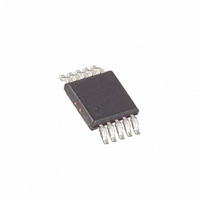
MAX3747BEUB+ Maxim Integrated Products, MAX3747BEUB+ Datasheet - Page 3

MAX3747BEUB+
Manufacturer Part Number
MAX3747BEUB+
Description
IC AMP LIMITING SFP 10-UMAX
Manufacturer
Maxim Integrated Products
Type
Limiting Amplifierr
Datasheet
1.MAX3747AEUB.pdf
(10 pages)
Specifications of MAX3747BEUB+
Applications
Data Quantizer, Optical Receivers
Mounting Type
Surface Mount
Package / Case
10-MSOP, Micro10™, 10-uMAX, 10-uSOP
Operating Supply Voltage
3.3 V
Supply Current
36 mA
Operating Temperature Range
+ 85 C
Available Set Gain
61 dB
Mounting Style
SMD/SMT
Number Of Channels
1
Power Dissipation
552 mW
Amplifier Type
Low Power
Supply Voltage Range
2.97V To 3.63V
Amplifier Case Style
µMAX
No. Of Pins
10
Termination Type
SMD
Rohs Compliant
Yes
Filter Terminals
SMD
Lead Free Status / RoHS Status
Lead free / RoHS Compliant
ELECTRICAL CHARACTERISTICS (continued)
(V
unless otherwise specified.) (Note 1)
Note 1:
Note 2:
Note 3:
Note 4:
Note 5:
Note 6:
Note 7:
Note 8:
Note 9:
Note 10: V
Input-Referred Noise
Low-Frequency Cutoff
LOS Hysteresis
LOS Assert/Deassert Time
Low LOS Assert Level
Low LOS Deassert Level
Medium LOS Assert Level
Medium LOS Deassert Level
High LOS Assert Level
High LOS Deassert Level
TTL/CMOS I/O
V
LOS Output High Voltage
LOS Output Low Voltage
DISABLE Input High
DISABLE Input Low
DISABLE Input Current
CC
REF
= +2.97V to +3.63V, CML output load is 50Ω to V
Voltage
The data-input transition time is controlled by a 4th-order Bessel filter with f
2.667Gbps and below. The f
Supply current is measured with unterminated outputs or with AC-coupled output termination (see Figure 1).
Between sensitivity and overload, all AC specifications are met and the output is 0.95 x limited output amplitude.
Guaranteed by design and characterization.
The deterministic jitter (DJ) caused by the input filter is not included in the DJ generation specification.
The PRBS 2
Random jitter was measured without using a filter at the input.
The signal at the input is switched between two amplitudes, Signal_ON and Signal_OFF, as shown in Figure 2A.
The signal at the input is switched between 1.2V
PARAMETER
TH
is the voltage at pin 5 referenced to V
_______________________________________________________________________________________
23
- 1 equivalent pattern consists of a K28.5 pattern plus 240 ones plus K28.5 pattern plus 240 zeros.
155Mbps to 3.2Gbps, Low-Power SFP
SYMBOL
-3db
V
V
V
V
V
REF
OH
OL
IH
IL
= 0.75 x 3.2GHz for a data rate of 3.2Gbps.
V
10log(V
MAX3747/MAX3747A (Notes 4, 8)
MAX3747B (Notes 4, 8, 9)
V
V
V
V
V
V
R
R
R
IN
TH
TH
TH
TH
TH
TH
LOS
LOS
LOS
CC
= 4mV
= -1.3V (Notes 4, 10)
= -1.3V (Notes 4, 10)
= -0.68V (Notes 4, 10)
= -0.68V (Notes 4, 10)
= -0.114V (Notes 4, 10)
= -0.114V (Notes 4, 10)
CC
(see Figure 5).
= 4.7k
= 4.7k
= 4.7k
DEASSERT
, T
P-P
A
P-P
and Signal_OFF as shown in Figure 2B.
= -40°C to +85°C. Typical values are at V
(Note 4)
to 10k
to 10k
to 10k
CONDITIONS
/ V
ASSERT
to V
to V
to V
CC_HOST
CC_HOST
CC_HOST
) (Note 4)
Limiting Amplifiers
-3dB
(3V)
(3.6V)
= 0.75 x 2.667GHz for all data rates of
V
1.25
22.0
36.0
1.35
MIN
2.3
2.5
2.4
2.0
CC
-
CC
V
TYP
29.0
44.8
53.7
86.0
1.3V
120
6.4
4.1
6.2
= +3.3V and T
CC
-
MAX
V
40.0
31.0
57.0
63.6
1.19
150
115
5.9
9.3
0.4
0.8
CC
10
-
A
= +25°C,
UNITS
μV
mV
mV
mV
mV
mV
mV
kHz
dB
μA
μs
RMS
V
V
V
V
V
P-P
P-P
P-P
P-P
P-P
P-P
3


