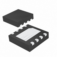
MAX3658AETA+T Maxim Integrated Products, MAX3658AETA+T Datasheet

MAX3658AETA+T
Specifications of MAX3658AETA+T
Related parts for MAX3658AETA+T
MAX3658AETA+T Summary of contents
Page 1
... Passive Optical Networks SFF/SFP Transceivers FTTx Transceivers Pin Configuration appears at end of data sheet. C FILT ________________________________________________________________ Maxim Integrated Products For pricing, delivery, and ordering information, please contact Maxim/Dallas Direct! at 1-888-629-4642, or visit Maxim’s website at www.maxim-ic.com. 622Mbps, Low-Noise, High-Gain Transimpedance Preamplifier ♦ 45nA RMS ♦ ...
Page 2
Low-Noise, High-Gain Transimpedance Preamplifier ABSOLUTE MAXIMUM RATINGS Supply Voltage (V ) ............................................-0.5V to +4.2V CC Current into IN ....................................................................+5mA Voltage at OUT+, OUT- ...................(V CC Voltage FILT, MON .....................................-0. Continuous Power Dissipation (T = +85°C) A 8-Lead ...
Page 3
AC ELECTRICAL CHARACTERISTICS (V = +2.97V to +3.63V, 150Ω load between OUT+ and OUT -40°C to +85°C. Typical values are design and characterization.) PARAMETER SYMBOL Bandwidth Input-Referred Noise Noise Density Low-Frequency Cutoff Deterministic ...
Page 4
Low-Noise, High-Gain Transimpedance Preamplifier (V = +3.3V 0.5pF +25°C, unless otherwise noted FILTER VOLTAGE vs. DC INPUT CURRENT 1600 1400 R = 500Ω 1200 FILT 1000 800 600 400 200 R = ...
Page 5
C = 0.5pF +25°C, unless otherwise noted OUTPUT EYE DIAGRAM (-28dBm OPTICAL INPUT) MAX3658 toc13 PRBS INPUT AT 622Mbps 300ps/div PIN NAME 1 V +3.3V Supply Voltage CC ...
Page 6
Low-Noise, High-Gain Transimpedance Preamplifier R f TIA IN MON FILT Detailed Description The MAX3658 transimpedance amplifier is designed for 622Mbps fiber optic applications. The MAX3658 is comprised of a transimpedance amplifier, a voltage amplifier, an output buffer ...
Page 7
AMPLITUDE INPUT FROM PHOTODIODE INPUT AFTER DC CANCELLATION Figure 2. DC Cancellation Effect on Input The output buffer is designed to drive a 150Ω differen- tial load between OUT+ and OUT-. For optimum supply noise rejection, the MAX3658 should be ...
Page 8
Low-Noise, High-Gain Transimpedance Preamplifier Select C so the low-frequency cutoff due to the COUPLE load resistors and coupling capacitors is much lower than the low-frequency cutoff of the MAX3658. The cou- pling capacitor should be 0.1µF or larger for ...
Page 9
P1 P AVG P0 TIME Figure 4. Optical Power Relations where ρ is the photodiode responsivity in A/W and i the RMS noise current in amps. For example, with pho- todiode responsivity of 0.9A/W, an extinction ratio of 10 and ...
Page 10
Low-Noise, High-Gain Transimpedance Preamplifier 75Ω MAX3658 OUTPUT STAGE *COMPONENT NOT REQUIRED IF L < 5cm Figure 6a. 50 Ω AC-Coupled Interface 75Ω MAX3658 OUTPUT STAGE NOTE: THE PARALLEL COMBINATION AT THE UNUSED OUTPUT CAN BE REPLACED BY A SINGLE ...
Page 11
V CC 400Ω 20kΩ FILT 20pF Figure 7. FILT Interface V CC MON Figure 8. MON Interface Pin Configuration TOP VIEW GND OUT- OUT MAX3658 AGP FILT MON CC TDFN* (3mm x ...
Page 12
Low-Noise, High-Gain Transimpedance Preamplifier MON 1 GND 2 N.C. 3 OUT+ 4 (0,0) 12 ______________________________________________________________________________________ FILT 0.029in 0.736mm Chip Topographies Topography for MAX3658A V CC GND 0.052in 1.32mm N.C. OUT- ...
Page 13
Low-Noise, High-Gain Transimpedance Preamplifier FILT MON 1 10 GND 2 N.C. 3 OUT- 4 (0,0) 0.029in 0.736mm ______________________________________________________________________________________ Chip Topographies (continued) Topography for MAX3658B GND N.C. 6 OUT+ 5 0.052in 1.32mm 13 ...
Page 14
Low-Noise, High-Gain Transimpedance Preamplifier (The package drawing(s) in this data sheet may not reflect the most current specifications. For the latest package outline information www.maxim-ic.com/packages.) COMMON DIMENSIONS MIN. MAX. SYMBOL A 0.70 0.80 D 2.90 3.10 E ...
Page 15
... Maxim cannot assume responsibility for use of any circuitry other than circuitry entirely embodied in a Maxim product. No circuit patent licenses are implied. Maxim reserves the right to change the circuitry and specifications without notice at any time. Maxim Integrated Products, 120 San Gabriel Drive, Sunnyvale, CA 94086 408-737-7600 ____________________ 15 © 2007 Maxim Integrated Products ...


