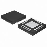
MAX3969ETP+ Maxim Integrated Products, MAX3969ETP+ Datasheet - Page 6

MAX3969ETP+
Manufacturer Part Number
MAX3969ETP+
Description
IC AMP LIMIT 200MBPS 20-TQFN
Manufacturer
Maxim Integrated Products
Type
Limiting Amplifierr
Datasheet
1.MAX3969ETP.pdf
(11 pages)
Specifications of MAX3969ETP+
Applications
Optical Networks
Mounting Type
Surface Mount
Package / Case
20-TQFN Exposed Pad
Operating Supply Voltage
3 V, 5 V
Supply Current
22 mA
Operating Temperature Range
+ 85 C
Mounting Style
SMD/SMT
Number Of Channels
1
Power Dissipation
1099 mW
Amplifier Type
Limiting
Supply Voltage Range
2.97V To 5.5V
Amplifier Case Style
TQFN
No. Of Pins
20
Termination Type
SMD
Rohs Compliant
Yes
Filter Terminals
SMD
Lead Free Status / RoHS Status
Lead free / RoHS Compliant
Each amplifier stage contains a logarithmic FWD, which
indicates the RMS input signal power. The FWD outputs
are summed together at the FILTER pin where the sig-
nal is filtered by an external capacitor (C
nected between FILTER and V
generates the RSSI output voltage (V
proportional to the input power in decibels. When LOS
is low, V
where, V
This relation translates to a 25mV increase in V
every 1dB increase in V
approximately 120mV when LOS is high.
Typically the RSSI output is connected to an A/D con-
verter for diagnostic monitoring. This output can be left
open if not required in the application. The RSSI output
is designed to drive a minimum load resistance of 10kΩ
to ground, and a maximum capacitance of 10pF. A
10kΩ series resistor is required to buffer loads greater
than 10pF.
A comparator is used to indicate the input signal
strength relative to a user-programmable threshold.
One of the comparator inputs is connected to the RSSI
output signal, and the other is connected to the thresh-
old voltage (V
a trip point for signal-strength indication. When the sig-
nal strength is above the threshold, the SD output
asserts high and the LOS output deasserts low.
Likewise, when the signal strength falls below the
threshold, SD deasserts low and LOS asserts high. To
ensure chatter-free operation, the comparator is
designed with approximately 5dB of hysteresis.
The squelch function disables the data outputs by forc-
ing OUT- low and OUT+ high when the input signal is
below the programmed threshold. This function
ensures that when there is a loss of signal, the limiting
amplifier and all downstream devices do not respond to
input noise. Connect SQUELCH to GND or leave it
unconnected to disable squelch. Connect SQUELCH to
V
200Mbps SFP Limiting Amplifier
6
CC
_______________________________________________________________________________________
to enable squelch.
RSSI
IN
is the data input voltage measured in mV
V
is approximated by the following equation:
RSSI
TH
), which is set externally and provides
(V) = 1.2V + 0.5log (V
Signal-Strength Comparator
IN
. The RSSI output is reduced
CC
. The FILTER signal
Power Detector
RSSI
IN
)
FILTER
), which is
Squelch
RSSI
) con-
P-P
for
.
The data outputs (OUT+, OUT-) and signal-detect out-
put (SD) are supply-referenced PECL outputs. See
Figure 2 for the equivalent output circuit.
Both data outputs must be terminated for proper opera-
tion, but the SD output can be left open if not required
in the application. The proper termination for a PECL
output is 50Ω to (V
tion techniques can be used. For more information on
PECL terminations and how to interface with other logic
families, refer to Maxim Application Note HFAN-01.0:
Introduction to LVDS, PECL, and CML.
The LOS outputs (LOS, LOS) are implemented with
open-collector, Schottky-clamped, ESD-protected, TTL-
compatible outputs. See Figure 3 for the equivalent out-
put circuit. The LOS outputs require external pullup
resistors for proper operation. Resistor values between
4.7kΩ and 10kΩ are recommended.
If the LOS outputs are not required for the application,
they can be left open.
The suggested procedure for setting the power-detect
threshold is given below and is illustrated in Figure 4.
1) Determine the maximum receiver sensitivity
2) Calculate the differential voltage swing (VIN_SEN) at
3) Calculate the threshold voltage (V
4) Use V
(RX_MAX) in dBm and the PIN-TIA responsivity (G)
in V/W.
the MAX3969 inputs while operating at sensitivity.
LOS must be low (SD must be high) by allowing
3.6dB (1.8dB optical) margin for power-detector
accuracy.
LOW) in the Power-Detect Threshold vs. R2 graph
in the Typical Operating Characteristics to deter-
mine the value of R2. Select R1=100kΩ.
Program the Power-Detect Threshold
IN_TH
V
IN_SEN
V
and the line labeled (SD HIGH / LOS
IN_TH
CC
= 10
- 2V), but other standard termina-
= V
(RX_MAX / 10)
IN_SEN
Design Procedure
x 0.66
x 2 x G
PECL Outputs
TTL Outputs
IN_TH
) at which


