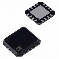
AD8305ACP-R2 Analog Devices Inc, AD8305ACP-R2 Datasheet - Page 3

AD8305ACP-R2
Manufacturer Part Number
AD8305ACP-R2
Description
IC LOGARITHM CONV 100DB 16-LFCSP
Manufacturer
Analog Devices Inc
Type
Logarithmic Converterr
Datasheet
1.AD8305ACPZ-RL7.pdf
(24 pages)
Specifications of AD8305ACP-R2
Rohs Status
RoHS non-compliant
Design Resources
Interfacing ADL5315 to Translinear Logarithmic Amplifier (CN0056) Interfacing ADL5317 High Side Current Mirror to a Translinear Logarithmic Amplifier in an Avalanche Photodiode Power Detector
Applications
Fiber Optics
Mounting Type
Surface Mount
Package / Case
16-LFCSP
Other names
AD8305ACP-R2CT
SPECIFICATIONS
V
Table 1.
Parameter
INPUT INTERFACE
LOGARITHMIC OUTPUT
REFERENCE OUTPUT
OUTPUT BUFFER
POWER SUPPLY
1
2
Other values of logarithmic intercept can be achieved by adjusting R
Output noise and incremental bandwidth are functions of input current, measured using output buffer connected for GAIN = 1.
P
Specified Current Range, I
Input Current Min/Max Limits
Reference Current, I
Summing Node Voltage
Temperature Drift
Input Offset Voltage
Logarithmic Slope
Logarithmic Intercept
Law Conformance Error
Wideband Noise
Small Signal Bandwidth
Maximum Output Voltage
Minimum Output Voltage
Output Resistance
Voltage With Reference to Ground
Maximum Output Current
Incremental Output Resistance
Input Offset Voltage
Input Bias Current
Incremental Input Resistance
Output Range
Incremental Output Resistance
Peak Source/Sink Current
Small Signal Bandwidth
Slew Rate
Positive Supply Voltage
Quiescent Current
Negative Supply Voltage (Optional)
= 5 V, V
N
= 0 V, T
2
A
REF
= 25°C, R
, Range
1
2
PD
REF
= 200 kΩ, and VRDZ connected to VREF, unless otherwise noted.
Conditions
Pin 4, INPT, Pin 3, IREF
Flows toward INPT pin
Flows toward INPT pin
Flows toward IREF pin
Internally preset; may be altered by the user
−40°C < T
V
Pin 9, VLOG
−40°C < T
−40°C < T
10 nA < I
I
I
Limited by V
Pin 2, VREF
−40°C < T
Sourcing (grounded load)
Pin 10, BFIN; Pin 11, SCAL; Pin 12, VOUT
Flowing out of Pin 10 or Pin 11
R
GAIN = 1
Pin 8, VPOS; Pin 6 and Pin 7, VNEG
(V
(V
Load current < 10 mA
Load current < 10 mA
0.2 V to 4.8 V output swing
PD
PD
INPT
L
P
P
= 1 kΩ to ground
> 1 μA
> 1 μA
− V
− V
− V
N
N
) ≤ 12 V
) ≤ 12 V
SUM
PD
A
A
A
A
, V
< +85°C
< +85°C
< +85°C
< 1 mA
< +85°C
N
REF
IREF
= 0 V
.
− V
Rev. B | Page 3 of 24
SUM
Min
10
10
0.46
−20
190
185
0.3
0.1
4.375
2.435
2.4
−20
3
−5.5
Typ
0.5
0.015
200
1
0.1
0.7
0.7
1.7
0.01
5
2.5
20
2
0.4
35
V
0.5
25
15
15
5
5.4
0
P
− 0.1
Max
1
10
1
0.54
+20
210
215
1.7
2.5
0.4
5.625
2.565
2.6
+20
12
6.5
AD8305
Unit
nA
mA
mA
nA
mA
V
mV/°C
mV
mV/dec
mV/dec
nA
nA
dB
mV√Hz
MHz
V
V
kΩ
V
V
mA
Ω
mV
mA
MΩ
V
Ω
mA
MHz
V/μs
V
mA
V


