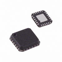
ADL5310ACP Analog Devices Inc, ADL5310ACP Datasheet - Page 16

ADL5310ACP
Manufacturer Part Number
ADL5310ACP
Description
IC LOGARITHMIC CONV DUAL 24LFCSP
Manufacturer
Analog Devices Inc
Type
Logarithmic Converterr
Datasheet
1.ADL5310ACPZ-REEL7.pdf
(20 pages)
Specifications of ADL5310ACP
Rohs Status
RoHS non-compliant
Design Resources
Interfacing ADL5315 to Translinear Logarithmic Amplifier (CN0056) Interfacing ADL5317 High Side Current Mirror to a Translinear Logarithmic Amplifier in an Avalanche Photodiode Power Detector
Applications
Fiber Optics
Mounting Type
Surface Mount
Package / Case
24-LFCSP
Available stocks
Company
Part Number
Manufacturer
Quantity
Price
Company:
Part Number:
ADL5310ACP-REEL7
Manufacturer:
TEXAS
Quantity:
550
Company:
Part Number:
ADL5310ACPZ
Manufacturer:
Analog Devices Inc
Quantity:
1 914
Part Number:
ADL5310ACPZ
Manufacturer:
ADI/亚德诺
Quantity:
20 000
Company:
Part Number:
ADL5310ACPZ-REEL7
Manufacturer:
CIRRUS
Quantity:
390
ADL5310
The solution in Figure 37 is no longer subject to potential
channel mismatch issues. Individual channel slope and intercept
characteristics can be calibrated independently. The accuracy
was verified using a pair of calibrated current sources. The
performance of the circuit depicted in Figure 37 is shown in
Figure 38 and Figure 39. Multiple transfer functions and error
plots are provided for various power levels. The accuracy is
better than 0.1 dB over a 5-decade range. The dynamic range is
slightly reduced for strong I
limited available swing of the VLOG pin and can be recovered
through careful selection of input and output optical tap
coupling ratios.
Figure 39. Log Conformance for Wilson Mirror ADL5310 Combination,
–0.1
–0.2
–0.3
–0.4
–0.5
Figure 38. Absorbance and Absolute Power Transfer Functions for
0.5
0.4
0.3
0.2
0.1
1.8
1.6
1.4
1.2
1.0
0.8
0.6
0.4
0.2
–20
–40
0
0
I
PD1
Normalized to 10 mA Channel 1 Input Current, I
–30
= 10µA
φ
–10
2
WHEN I
I
PD1
–20
Wilson Mirror ADL5310 Combination
= 1µA
0
PD1
–10
= 100µA
LOG
LOG
I
10
PD1
0
10
10
IN
α
= 100µA
[I
21
[I
input currents. This is due to the
PD1
PD1
FOR MULTIPLE VALUES OF I
20
10
/I
/I
PD2
PD2
20
] (dB)
] (dB)
30
30
40
40
50
50
IN1
PD1
60
60
Rev. A | Page 16 of 20
CHARACTERIZATION METHODS
During the characterization of the ADL5310, the device was
treated as a precision current-input logarithmic converter,
because it is impractical to generate accurate photocurrents by
illuminating a photodiode. The test currents were generated by
using either a well-calibrated current source, such as the
Keithley 236, or a high value resistor from a voltage source to
the input pin. Great care is needed when using very small input
currents. For example, the triax output connection from the
current generator was used with the guard tied to VSUM. The
input trace on the PC board was guarded by connecting
adjacent traces to VSUM.
These measures are needed to minimize the risk of leakage
current paths. With 0.5 V as the nominal bias on the INP1
(INP2) pin, a leakage-path resistance of 1 GΩ to ground would
subtract 0.5 nA from the input, which amounts to a −1.6 dB
error for a 3 nA source current. Additionally, the very high
sensitivity at the input pins and the long cables commonly
needed during characterization allow 60 Hz and RF emissions
to introduce substantial measurement errors. Careful guarding
techniques are essential to reducing the pickup of these spurious
signals.
Additional information, including test setups, can be found in
the AD8305 and ADL5306 data sheets.


