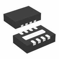
LT6552IDD#PBF Linear Technology, LT6552IDD#PBF Datasheet - Page 11

LT6552IDD#PBF
Manufacturer Part Number
LT6552IDD#PBF
Description
IC AMP VIDEO DIFF 3.3V 8-DFN
Manufacturer
Linear Technology
Datasheet
1.LT6552CS8PBF.pdf
(16 pages)
Specifications of LT6552IDD#PBF
Applications
Differential
Number Of Circuits
1
-3db Bandwidth
75MHz
Slew Rate
600 V/µs
Current - Supply
14mA
Current - Output / Channel
70mA
Voltage - Supply, Single/dual (±)
3 V ~ 12.6 V, ±1.5 V ~ 6.3 V
Mounting Type
Surface Mount
Package / Case
8-WFDFN Exposed Pad
Lead Free Status / RoHS Status
Lead free / RoHS Compliant
Available stocks
Company
Part Number
Manufacturer
Quantity
Price
APPLICATIO S I FOR ATIO
The LT6552 is a video difference amplifier with two pairs
of high impedance inputs. The primary purpose of the
LT6552 is to convert high frequency differential signals
into a single-ended output, while rejecting any common
mode noise. In the simplest configuration, one pair of
inputs is connected to the incoming differential signal,
while the other pair of inputs is used to set amplifier gain
and DC level. The device will operate on either single or
dual supplies and has an input common mode range
which includes the negative supply. The common mode
rejection ratio is greater than 60dB at 10MHz. Feedback is
U
V
IN
U
3
2
1
8
R
G
SHDN
+
–
FB
REF
LT6552
V
5
O
V
V
= +
R
+
–
7
4
F
(
R
W
F
R
+ R
G
6
G
(
V
V
IN
O
V
INDIFF
U
V
DC
V
IN
3
2
1
8
R
3
2
1
8
R
G
SHDN
+
–
FB
V
REF
G
SHDN
O
+
–
FB
REF
Figure 3
LT6552
Figure 4
= (V
5
LT6552
V
5
V
O
R
INDIFF
V
V
+
R
= –
7
4
F
+
–
7
4
F
applied to Pin 8 and the LT6552’s transient response is
optimized for gains of 2 or greater.
Figure 3 shows the single supply connection. The ampli-
fier gain is set by a feedback network from the output to
Pin 8 (FB). A DC signal applied to Pin 1 (REF) establishes
the output quiescent voltage and the differential signal is
applied to Pins 2 and 3.
Figure 4 shows several other connections using dual
supplies. In each case, the amplifier gain is set by a
feedback network from the output to Pin 8 (FB).
(
R
+ V
F
R
6
+ R
DC
G
6
)
G
R
6552 F01
(
V
F
V
O
R
V
V
+ R
IN
IN
G
O
G
V
R
INDIFF
G
V
O
=
(
R
3
2
1
8
F
R
+ R
G
SHDN
+
–
FB
REF
LT6552
G
5
(
V
V
V
R
INDIFF
–
+
7
4
F
–
( (
6
R
R
G
F
6552 F01
V
V
IN
O
LT6552
11
6552f


