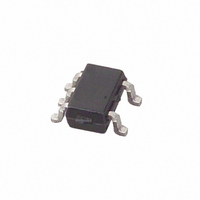
MAX9502GEXK+T Maxim Integrated Products, MAX9502GEXK+T Datasheet - Page 8

MAX9502GEXK+T
Manufacturer Part Number
MAX9502GEXK+T
Description
IC VIDEO AMP W/FILTER SC70-5
Manufacturer
Maxim Integrated Products
Datasheet
1.MAX9502GEXKT.pdf
(11 pages)
Specifications of MAX9502GEXK+T
Applications
Reconstruction Filter
Number Of Circuits
1
Current - Supply
5.3mA
Current - Output / Channel
95mA
Voltage - Supply, Single/dual (±)
2.5 V ~ 3.6 V
Mounting Type
Surface Mount
Package / Case
6-TSSOP (5 lead), SC-88A, SOT-353
Number Of Channels
1
Operating Supply Voltage
2.5 V
Supply Current
7 uA
Minimum Operating Temperature
- 40 C
Maximum Operating Temperature
+ 85 C
Maximum Dual Supply Voltage
5.25 V
Minimum Dual Supply Voltage
2 V
Supply Voltage (max)
3.6 V
Supply Voltage (min)
2.5 V
Lead Free Status / RoHS Status
Lead free / RoHS Compliant
Other names
MAX9502GEXK+TTR
The MAX9502 filters and amplifies the video DAC output
in applications such as digital still cameras and mobile
phones. The MAX9502 consists of a lowpass filter and an
output video buffer capable of driving a standard 150Ω
video load to ground. The MAX9502G output buffer pro-
vides a fixed gain of +6dB, while the MAX9502M output
buffer provides a fixed gain of +12dB.
The MAX9502 contains a 4th-order Chebyshev recon-
struction filter. The Chebyshev-type response features
a 0.4dB flat passband for NTSC and PAL signals. The
stopband offers 55dB (typ) of attenuation at 27MHz
and above (see the Typical Operating Characteristics).
The MAX9502G features a +6dB gain, while the
MAX9502M features a +12dB gain. Operating from a
2.5V to 3.0V supply, the output amplifier is able to drive a
2V signal into a 150Ω video load to ground. Operating
from a 3.0V to 3.6V supply, the output amplifier is able to
drive a 2.4V
The output is typically offset 110mV above ground to
guarantee linear operation of the amplifier. The MAX9502
output only sources current; all loads should be connect-
ed to ground.
The MAX9502 typical application circuit includes a 75Ω
back-termination resistor that limits short-circuit currents
for an external short applied at the video output. The
MAX9502 features internal output short-circuit protection
to prevent device damage in prototyping and applica-
tions where the amplifier output can be directly shorted.
Short-circuit protection activates if the output is short-cir-
cuited and the output current exceeds 95mA. During
short-circuit protection, the output of the MAX9502 is shut
off for 12µs and then turns on for 0.8µs. If the short is still
present, the MAX9502 output shuts off again. Extended
short circuits result in a pulsed output. The device
resumes normal operation after the short is removed.
2.5V Video Amplifier with Reconstruction Filter
8
_______________________________________________________________________________________
P-P
signal into a 150Ω video load to ground.
Detailed Description
Short-Circuit Protection
Output Amplifier
Filter
The MAX9502 input is DC-coupled. When the supply
voltage is between a 2.5V and 3V supply, the input volt-
age range extends from ground to 1.05V for the
MAX9502G and from ground to 0.525V for the
MAX9502M. When the supply voltage is between 3V and
3.6V, the input voltage range extends from ground to
1.2V for the MAX9502G and from ground to 0.6V for the
MAX9502M. The MAX9502G accepts a composite video
signal with a sync tip from 0 to 50mV and the MAX9502M
accepts a composite video signal with a sync tip from 0
to 25mV. A typical current-output DAC that operates
from a single supply usually creates a composite video
signal with a sync tip very close to ground. Hence, the
DAC output can be directly connected to the MAX9502
input. Keep the board trace as short as possible to mini-
mize parasitic stray capacitance and prevent uninten-
tional high-frequency attenuation.
The MAX9502 output must be DC-coupled. No AC-cou-
pling capacitors are allowed. The MAX9502 connects
directly to the video cable through a 75Ω series back-
termination resistor. The other end of the cable should
be properly terminated with a 75Ω resistor as well.
Because of this configuration, the peak-to-peak ampli-
tude as well as the DC level of the signal is divided by
two. The MAX9502 output signal is level-shifted up so
the sync tip is around 110mV.
The MAX9502 operates from a single-supply voltage
down to 2.5V, allowing for low-power consumption.
Bypass V
external components as close to the device as possible.
Power-Supply Bypassing and Layout
CC
to GND with a 0.1µF capacitor. Place all
Applications Information
Output Considerations
Input Considerations
Considerations


