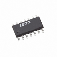
ZXFV201N14TA Diodes Zetex, ZXFV201N14TA Datasheet - Page 2

ZXFV201N14TA
Manufacturer Part Number
ZXFV201N14TA
Description
IC AMPLIFIER VIDEO QUAD 14-SOIC
Manufacturer
Diodes Zetex
Specifications of ZXFV201N14TA
Applications
Current Feedback
Number Of Circuits
4
-3db Bandwidth
210MHz
Slew Rate
600 V/µs
Current - Supply
7.5mA
Current - Output / Channel
40mA
Voltage - Supply, Single/dual (±)
±4.75 V ~ 5.25 V
Mounting Type
Surface Mount
Package / Case
14-SOIC (0.154", 3.90mm Width)
Single Supply Voltage (typ)
Not RequiredV
Dual Supply Voltage (typ)
±5V
Single Supply Voltage (min)
Not RequiredV
Single Supply Voltage (max)
Not RequiredV
Operating Temperature Classification
Industrial
Mounting
Surface Mount
For Use With
ZXFV201EV - BOARD EVAL FOR QUAD VIDEO AMP
Lead Free Status / RoHS Status
Contains lead / RoHS non-compliant
Other names
ZXFV201N14TR
ABSOLUTE MAXIMUM RATINGS Over Operating Free-Air Temperature (Unless Otherwise Stated
Supply voltage, V+ to V-
Input voltage (V
Differential input voltage, VID
Inverting input current (I-IN)
Output current, (continuous, T
Internal power dissipation
Operating free air temperature range, T
Storage temperature range
Operating ambient junction temperature T
Notes:
(1) Stresses above those listed under Absolute Maximum Ratings may cause permanent damage to the device. This is a stress rating only;
(2) At high closed loop gains and low gain setting resistors care must be taken if large input signals are applied to the device which cause the
(3) The power dissipation of the device when loaded must be designed to keep the device junction temperature below T
*During power-up and power-down, these voltage ratings require that signals be applied only when the power supply is connected.
ESD: This device is sensitive to static discharge and proper handling precautions are required.
ELECTRICAL CHARACTERISTICS
±5V power supplies, T
Test – P = production tested. C = characterised
ZXFV201, ZXFV203
PARAMETER
Supply voltage V+ operating range
Supply voltage V- operating range
Supply current/per channel
Input common mode voltage range
Input offset voltage
Output offset voltage
Input bias current, non-inverting input
Input resistance
Output voltage swing
Output drive current
Positive PSRR
Negative PSRR
Bandwidth –3dB
Bandwidth –0.1dB
Slew rate
Rise time
Fall time
Propagation delay
Differential gain
Differential phase
functional operation of the device at these or any other conditions above those indicated in the operational section of this specification is not
implied. Exposure to absolute maximum rating conditions for extended periods may affect device reliability.
output stage to saturate for extended periods of time.
S E M I C O N D U C T O R S
-IN
, V
+IN
amb
)*
Package
SO14
= 25°C unless otherwise stated. R
(2)
J
< 110°C)
Theta-ja
120°C/W
A
CONDITIONS
I
V
Av= +1, Vout = 200mV pk-pk C
Av= +1, Vout = 200mV pk-pk C
Av= +1
Av = +2
Av = +10
V
V
V
3.58MHz (NTSC) and
4.43MHz (PAL) DC = -714 to
+714 mV, 280mVpp
OUT
IN
V+ = ±0.25
V- = ±0.25
OUT
OUT
OUT
JMAX
= 3V
= 40mA
=
=
=
-0.5V to +11V
V
±3V
±5 mA
±60 mA
See power dissipation derating table
-40 to 85°C
-65°C to +150°C
150°C
Power rating at 25°C
1.04W
-
1 V, 10% - 90%
1 V, 10% - 90%
2 V, 50%
-0.5V to V
2
f
= 1k , R
+
+0.5V
L
= 150 , C
TEST MIN
P
P
P
P
P
P
P
P
P
P
C
C
C
C
C
C
-5.25
L
4.75
5.0
1.5
40
49
49
= 10pF
ISSUE 3 - DECEMBER 2003
0.02
0.02
TYP
300
400
400
400
7.5
4.0
3.2
4.0
57
57
30
-5
5
1
2
5
2
3
3
JMAX
MAX
-4.75
.
5.25
6.5
10
10
20
10
UNIT
V/ s
MHz
MHz
deg
mA
mV
mV
M
mA
dB
dB
ns
ns
ns
%
V
V
V
V
A
(1)


