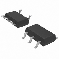
LT6205HS5#TRMPBF Linear Technology, LT6205HS5#TRMPBF Datasheet

LT6205HS5#TRMPBF
Specifications of LT6205HS5#TRMPBF
Available stocks
Related parts for LT6205HS5#TRMPBF
LT6205HS5#TRMPBF Summary of contents
Page 1
... SSOP package. These devices are specifi ed over the commercial, industrial and automotive temperature ranges. L, LT, LTC, LTM, Linear Technology and the Linear logo are registered trademarks and ThinSOT is a trademark of Linear Technology Corporation. All other trademarks are the property of their respective owners. V OUT1 75Ω ...
Page 2
LT6205/LT6206/LT6207 ABSOLUTE MAXIMUM RATINGS + – Total Supply Voltage ( ..............................12.6V Input Current .......................................................±10mA Input Voltage Range (Note 2) ....................................±V Output Short-Circuit Duration (Note 3) ........... Indefi nite Pin Current While Exceeding Supplies (Note 9) ...±25mA Operating ...
Page 3
ELECTRICAL CHARACTERISTICS range, otherwise specifi cations are SYMBOL PARAMETER V Input Offset Voltage OS Input Offset Voltage Match (Channel-to-Channel) (Note 5) Input Offset Voltage Drift (Note 6) I Input Bias Current B I Input Offset Current OS ...
Page 4
LT6205/LT6206/LT6207 ELECTRICAL CHARACTERISTICS range, otherwise specifi cations are SYMBOL PARAMETER V Input Offset Voltage OS Input Offset Voltage Match (Channel-to-Channel) (Note 5) Input Offset Voltage Drift (Note 6) I Input Bias Current B I Input Offset Current ...
Page 5
ELECTRICAL CHARACTERISTICS range, –40°C ≤ T ≤ 125°C, otherwise specifi cations are SYMBOL PARAMETER I Input Offset Current OS Input Noise Voltage e Input Noise Voltage Density n i Input Noise Current Density n Input Resistance Input ...
Page 6
LT6205/LT6206/LT6207 ELECTRICAL CHARACTERISTICS temperature range, –40°C ≤ T ≤ 125°C, otherwise specifi cations are SYMBOL PARAMETER I Input Bias Current B I Input Offset Current OS Input Noise Voltage e Input Noise Voltage Density n i Input ...
Page 7
TYPICAL PERFORMANCE CHARACTERISTICS V Distribution 5V –3 –2 – INPUT OFFSET VOLTAGE (mV) 620567 G01 Change in Offset Voltage ...
Page 8
LT6205/LT6206/LT6207 TYPICAL PERFORMANCE CHARACTERISTICS Short-Circuit Current vs Temperature SINKING 70 SOURCING –50 – 100 TEMPERATURE (°C) 620567 G10 Warm Up Drift vs Time (LT6206) 120 T ...
Page 9
TYPICAL PERFORMANCE CHARACTERISTICS Gain Bandwidth and Phase Margin vs Temperature 5pF S L PHASE MARGIN 120 S 110 V = 3V, 0V 100 ...
Page 10
LT6205/LT6206/LT6207 TYPICAL PERFORMANCE CHARACTERISTICS Series Output Resistor vs Capacitive Load 5V 25° 10Ω 20Ω ...
Page 11
TYPICAL PERFORMANCE CHARACTERISTICS Large Signal Response V = ± 50ns/DIV 620567 G37 V = ± 150Ω L APPLICATIONS INFORMATION DESD1 150Ω Q1 +IN DESD2 D1 ...
Page 12
LT6205/LT6206/LT6207 APPLICATIONS INFORMATION Amplifi er Characteristics Figure 1 shows a simplifi ed schematic of the LT6205/ LT6206/LT6207. The input stage consists of transistors and resistor R1. This topology allows for high slew rates at low supply voltages. ...
Page 13
APPLICATIONS INFORMATION black intensity, thereby causing scan retrace activity to be invisible on a CRT. The black level of the waveform is at (or set up very slightly above) the upper limit of the sync information. Waveform content above the ...
Page 14
LT6205/LT6206/LT6207 TYPICAL APPLICATION COMPOSITE VIDEO IN 1V P-P 14 3.3V 0.1μ 2. – 4.7μF LT6205 BAT54 10k C2 470Ω 4.7μF 620567 TA02 Figure 2. Clamped AC-Input Video Cable Driver 75Ω VIDEO ...
Page 15
PACKAGE DESCRIPTION 0.62 MAX 3.85 MAX 2.62 REF RECOMMENDED SOLDER PAD LAYOUT PER IPC CALCULATOR 0.20 BSC DATUM ‘A’ 0.30 – 0.50 REF NOTE: 1. DIMENSIONS ARE IN MILLIMETERS 2. DRAWING NOT TO SCALE 3. DIMENSIONS ARE INCLUSIVE OF PLATING ...
Page 16
LT6205/LT6206/LT6207 PACKAGE DESCRIPTION 0.42 ± 0.038 (.0165 ± .0015) TYP RECOMMENDED SOLDER PAD LAYOUT GAUGE PLANE 0.18 (.007) NOTE: 1. DIMENSIONS IN MILLIMETER/(INCH) 2. DRAWING NOT TO SCALE 3. DIMENSION DOES NOT INCLUDE MOLD FLASH, PROTRUSIONS OR GATE BURRS. MOLD ...
Page 17
... C Grade Specifi ed Temperature Range Changed in the Order Information Section Information furnished by Linear Technology Corporation is believed to be accurate and reliable. However, no responsibility is assumed for its use. Linear Technology Corporation makes no representa- tion that the interconnection of its circuits as described herein will not infringe on existing patent rights. ...
Page 18
... B 107Ω 150Ω 75Ω 80.6Ω 499Ω 150Ω 150Ω G 75Ω 1.4 • 1.8 • – 0.34 • P – 0.71 • P 620567 TA03 B R 620567fc LT 0310 REV C • PRINTED IN USA © LINEAR TECHNOLOGY CORPORATION 2003 ...


