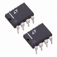
LT1187CN8 Linear Technology, LT1187CN8 Datasheet - Page 8

LT1187CN8
Manufacturer Part Number
LT1187CN8
Description
IC AMP VIDEO DIFFRNC ADJ 8-DIP
Manufacturer
Linear Technology
Datasheet
1.LT1187CS8PBF.pdf
(16 pages)
Specifications of LT1187CN8
Applications
Differential
Number Of Circuits
1
-3db Bandwidth
50MHz
Slew Rate
165 V/µs
Current - Supply
13mA
Current - Output / Channel
20mA
Voltage - Supply, Single/dual (±)
4.75 V ~ 16 V, ±2.38 V ~ 8 V
Mounting Type
Through Hole
Package / Case
8-DIP (0.300", 7.62mm)
Power Supply Requirement
Single/Dual
Dual Supply Voltage (typ)
±5V
Mounting
Through Hole
Pin Count
8
Lead Free Status / RoHS Status
Contains lead / RoHS non-compliant
Lead Free Status / RoHS Status
Contains lead / RoHS non-compliant
Available stocks
Company
Part Number
Manufacturer
Quantity
Price
Part Number:
LT1187CN8#PBF
Manufacturer:
LINEAR/凌特
Quantity:
20 000
APPLICATIONS INFORMATION
LT1187
The primary use of the LT1187 is in converting high speed
differential signals to a single-ended output. The LT1187
video difference amplifi er has two uncommitted high
input impedance (+) and (–) inputs. The amplifi er has
another set of inputs which can be used for reference and
feedback. Additionally, this set of inputs give gain adjust
and DC control to the difference amplifi er. The voltage
gain of the LT1187 is set like a conventional operational
amplifi er. Feedback is applied to Pin 8, and it is optimized
for gains of 2 or greater. The amplifi er can be operated
single-ended by connecting either the (+) or (–) inputs to
the +/REF (Pin 1). The voltage gain is set by the resistors:
(R
Like the single-ended case, the differential voltage gain is
set by the external resistors: (R
input differential signal for which the output will respond
is approximately ±0.38V.
V
8
IN DIFF
V
IN
FB
V
IN
+ R
3
2
1
8
3
2
1
8
R
R
G
G
G
+
–
–/FB
+
–
–/FB
+/REF
+/REF
S/D
S/D
)/R
LT1187
LT1187
V
5
5
A
O
V
V
V
R
V
V
R
G
= (V
+
–
FB
= +
+
–
FB
7
4
7
4
.
IN DIFF
R
FB
R
+
G
6
6
R
+ V
G
IN
V
V
)
OUT
OUT
R
FB
R
V
+
G
IN
R
G
FB
V
R
IN DIFF
G
V
V
+ R
O
IN
=
G
(
R
)/R
3
2
1
8
R
FB
3
2
1
8
G
R
+
–
+
+/REF
–/FB
G
+
–
S/D
–/FB
+/REF
R
S/D
G
LT1187
G
LT1187
5
. The maximum
A
5
(
V
V
V
V
R
R
V
V
= –
IN DIFF
+
–
FB
7
4
FB
+
–
7
4
R
FB
R
–
+
G
( (
6
R
R
6
R
LT1187 • AI01
FB
G
G
V
V
V
OUT
IN
OUT
Power Supply Bypassing
The LT1187 is quite tolerant of power supply bypassing.
In some applications a 0.1µF ceramic disc capacitor placed
1/2 inch from the amplifi er is all that is required. In ap-
plications requiring good settling time, it is important to
use multiple bypass capacitors. A 0.1µF ceramic disc in
parallel with a 4.7µF tantalum is recommended.
Calculating the Output Offset Voltage
Both input stages contribute to the output offset voltage at
Pin 6. The feedback correction forces balance in the input
stages by introducing an input V
expression for the output offset voltage is:
V
R
and R
DC reference voltage, for V
I
simplifi es to:
If R
tributes only 2mV, since I
OS
OUT
S
3
V
R
represents the input source resistance, typically 75Ω,
+
FB
is normally a small contributor and the expression
OUT
S
= (V
REF
is limited to 1k the last term of the equation con-
2
= V
R
OS
–
represents the fi nite source impedance from the
S
Figure 1. Simplifi ed Input Stage Schematic
Q1
OS
+ I
345 A
1.1k
(R
OS
R
E
FB
(R
Q2
S
+ R
) + I
G
+
B
)/R
(R
1 REF
B
R
REF
G
REF
is less than 2µA.
REF
+ I
)) • (R
grounded, R
Q3
B
OS
350 A
(R
1.1k
R
E
at Pin 8. The complete
FB
FB
Q4
)
+ R
G
7 V
4 V
)/R
REF
8
+
–
G
= 0Ω. The
+ I
R
B
G
ILT1187 • F01
(R
R
FB
6
1187fa
FB
)


