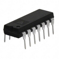
AD813ANZ Analog Devices Inc, AD813ANZ Datasheet - Page 16

AD813ANZ
Manufacturer Part Number
AD813ANZ
Description
IC OPAMP TRIPLE VIDEO LP 14DIP
Manufacturer
Analog Devices Inc
Datasheet
1.AD813ARZ-14.pdf
(19 pages)
Specifications of AD813ANZ
Slew Rate
250 V/µs
Applications
Current Feedback
Number Of Circuits
3
-3db Bandwidth
100MHz
Current - Supply
4.5mA
Current - Output / Channel
50mA
Voltage - Supply, Single/dual (±)
2.4 V ~ 36 V, ±1.2 V ~ 18 V
Mounting Type
Through Hole
Package / Case
14-DIP (0.300", 7.62mm)
Gain Bandwidth
125MHz
Supply Voltage Range
2.4V To 36V
No. Of Amplifiers
3
Output Current
50mA
Amplifier Output
Single Ended
Operating Temperature Range
-40°C To +85°C
Lead Free Status / RoHS Status
Lead free / RoHS Compliant
Available stocks
Company
Part Number
Manufacturer
Quantity
Price
Company:
Part Number:
AD813ANZ
Manufacturer:
MAXIM
Quantity:
17 513
AD813
High Performance Video Line Driver
At a gain of +2, the AD813 makes an excellent driver for a back
terminated 75
errors and wide 0.1 dB bandwidth can be realized over a wide
range of power supply voltage. Excellent gain and group delay
matching are also attainable over the full operating supply volt-
age range.
Figure 47. Closed-Loop Gain & Phase vs. Frequency for
the Line Driver
Figure 46. A Video Line Driver Operating at a Gain of
+2 (R
Figure 48. –3 dB Bandwidth vs. Supply Voltage for
Gain = +2, R
V
IN
120
110
100
90
80
70
60
50
40
30
20
–1
–2
–3
–4
–5
–6
+1
0
F
0
CABLE
1
= R
75
PHASE
GAIN
G
2
R
G
from Table I)
video line. Low differential gain and phase
L
75
4
= 150
AD813
SUPPLY VOLTAGE – Volts
6
10
+V
–V
FREQUENCY – MHz
11
4
S
S
8
R
F
3V
0.1 F
0.1 F
5V
5V
10
3V
12
NO PEAKING
100
75
V
V
14
S
S
=
=
CABLE
5V
G = +2
R
15V
15V
16
75
R
R
R
L
F
F
F
= 150
5V
= 590
= 681
= 750
18
75
1000
20
V
+90
0
–180
–270
–90
OUT
–16–
Figures 50 and 51 show the worst case matching; the match
between amplifiers 2 and 3 is typically much better than this.
Figure 51. Group Delay and Group Delay Matching vs.
Frequency, G = +2, R
Figure 49. Fine-Scale Gain (Normalized) vs. Frequency
Figure 50. Closed-Loop Gain Matching vs. Frequency
–0.2
–0.3
–0.4
–0.5
–0.1
–0.5
–1.0
–0.5
–1.0
–1.5
–2.0
–2.5
0.2
0.1
2.5
2.0
1.5
1.0
0.5
1.0
0.5
10
0
0
100k
8
6
4
2
0
100k
1
G = +2
R
L
= 150
L
1M
1M
10
= 150
DELAY MATCHING
FREQUENCY – MHz
FREQUENCY – Hz
FREQUENCY – Hz
V
S
= 3V
V
DELAY
S
= 3V
V
S
10M
10M
100
=
5V
3V
5V
15V
V
G = +2
R
15V
5V
S
15V
L
=
= 150
3V
5V
15V
100M
100M
1000
REV. B


