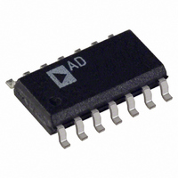
AD8013AR-14 Analog Devices Inc, AD8013AR-14 Datasheet - Page 3

AD8013AR-14
Manufacturer Part Number
AD8013AR-14
Description
IC OPAMP SINGLE SUPPLY 14-SOIC
Manufacturer
Analog Devices Inc
Datasheet
1.AD8013ARZ-14.pdf
(12 pages)
Specifications of AD8013AR-14
Slew Rate
1000 V/µs
Mounting Type
Surface Mount
Rohs Status
RoHS non-compliant
Applications
Current Feedback
Number Of Circuits
3
-3db Bandwidth
140MHz
Current - Supply
3.5mA
Current - Output / Channel
30mA
Voltage - Supply, Single/dual (±)
4.2 V ~ 13 V, ±2.1 V ~ 6.5 V
Package / Case
14-SOIC (0.154", 3.90mm Width)
No. Of Amplifiers
3
Bandwidth
280MHz
Amplifier Case Style
SOIC
No. Of Pins
14
Settling Time
18ns
Operating Temperature Max
85°C
Lead Free Status / RoHS Status
Contains lead / RoHS non-compliant
Available stocks
Company
Part Number
Manufacturer
Quantity
Price
Company:
Part Number:
AD8013AR-14
Manufacturer:
AD
Quantity:
46
Company:
Part Number:
AD8013AR-14
Manufacturer:
ADI
Quantity:
297
Part Number:
AD8013AR-14
Manufacturer:
ADI/亚德诺
Quantity:
20 000
Company:
Part Number:
AD8013AR-14-REEL
Manufacturer:
LT
Quantity:
124
Part Number:
AD8013AR-14-REEL
Manufacturer:
ADI/亚德诺
Quantity:
20 000
Model
POWER SUPPLY
DISABLE CHARACTERISTICS
NOTES
1
Specifications subject to change without notice.
Model
AD8013AN
AD8013AR-14
AD8013AR-14-REEL
AD8013AR-14-REEL7 –40 C to +85 C 14-Pin Plastic SOIC R-14
AD8013ACHIPS
REV. A
The test circuit for differential gain and phase measurements on a +5 V supply is ac coupled.
ABSOLUTE MAXIMUM RATINGS
Supply Voltage . . . . . . . . . . . . . . . . . . . . . . . . . . 13.2 V Total
Internal Power Dissipation
Input Voltage (Common Mode) . . Lower of V
Differential Input Voltage . . . . . . . . Output
Output Voltage Limit
Output Short Circuit Duration
Storage Temperature Range
Operating Temperature Range
Lead Temperature Range (Soldering 10 sec) . . . . . . . . +300 C
NOTES
1
2
Stresses above those listed under “Absolute Maximum Ratings” may cause
permanent damage to the device. This is a stress rating only and functional
operation of the device at these or any other conditions above those indicated in
the operational section of this specification is not implied. Exposure to absolute
maximum rating conditions for extended periods may affect device reliability.
Specification is for device in free air:
14-Pin Plastic DIP Package:
14-Pin SOIC Package:
Operating Range
Quiescent Current/Amplifier
Quiescent Current/Amplifier
Power Supply Rejection Ratio
Off Isolation
Off Output Impedance
Turn-On Time
Turn-Off Time
Switching Threshold
Plastic (N) . . . . . . . . . 1.6 Watts (Observe Derating Curves)
Small Outline (R) . . . . 1.0 Watts (Observe Derating Curves)
Maximum . . . . . . . . . Lower of (+12 V from –V
Minimum . . . . . . . . . Higher of (–12.5 V from +V
N and R Package . . . . . . . . . . . . . . . . . . . –65 C to +125 C
AD8013A . . . . . . . . . . . . . . . . . . . . . . . . . . –40 C to +85 C
Input Offset Voltage
–Input Current
+Input Current
. . . . . . . . . . . . . . . . . . . . Observe Power Derating Curves
JA
= 120 C/Watt
Temperature
Range
–40 C to +85 C 14-Pin Plastic DIP
–40 C to +85 C 14-Pin Plastic SOIC R-14
–40 C to +85 C 14-Pin Plastic SOIC R-14
–40 C to +85 C Die Form
ORDERING GUIDE
JA
2
= 75 C/Watt
1
Package
Description
Conditions
Single Supply
Dual Supply
Power Down
V
f = 6 MHz
G = +1
S
= 2.5 V to 5 V
6 V (Clamped)
S
or 12.25 V
S
S
) or (+V
) or (–V
Package
Options
N-14
S
S
)
)
–3–
Maximum Power Dissipation
The maximum power that can be safely dissipated by the AD8013
is limited by the associated rise in junction temperature. The
maximum safe junction temperature for the plastic encapsulated
parts is determined by the glass transition temperature of the
plastic, about 150 C. Exceeding this limit temporarily may
cause a shift in parametric performance due to a change in the
stresses exerted on the die by the package. Exceeding a junction
temperature of 175 C for an extended period can result in
device failure.
While the AD8013 is internally short circuit protected, this may
not be enough to guarantee that the maximum junction temper-
ature is not exceeded under all conditions. To ensure proper
operation, it is important to observe the derating curves.
It must also be noted that in (noninverting) gain configurations
(with low values of gain resistor), a high level of input overdrive
can result in a large input error current, which may result in a
significant power dissipation in the input stage. This power
must be included when computing the junction temperature rise
due to total internal power.
Maximum Power Dissipation vs. Ambient Temperature
V
+5 V
+5 V
+5 V, 5 V
+5 V, 5 V
+5 V, 5 V
+5 V, 5 V
–V
S
5 V
6.5 V
5 V
2.5
2.0
1.5
1.0
0.5
S
–50
+ xV
–40 –30 –20
14-PIN SOIC
AMBIENT TEMPERATURE – C
–10
Min
+4.2
70
1.3
2.1
0
10 20
AD8013A
14-PIN DIP PACKAGE
Typ
3.0
3.4
3.5
0.25
0.3
76
0.03
0.07
–70
12
50
30
1.6
30 40 50
Max
+13
3.5
4.0
0.35
0.4
0.2
1.0
1.9
T
J
6.5
= +150 C
60 70
AD8013
80
V
V
mA
mA
mA
mA
mA
dB
dB
pF
ns
ns
V
Units
A/V
A/V
90


