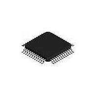
TSL1018IFT STMicroelectronics, TSL1018IFT Datasheet

TSL1018IFT
Specifications of TSL1018IFT
Available stocks
Related parts for TSL1018IFT
TSL1018IFT Summary of contents
Page 1
Features ■ Wide supply voltage: 5.5V to 16.8V ■ Low operating current: 8mA typical at 25°C ■ Bandwidth at -3dB: 3.5MHz ■ High output current COM amplifier: ±150mA ■ Industrial temperature range: -40°C to +95°C ■ Small package: TQFP48 ePad ...
Page 2
Absolute maximum ratings and operating conditions 1 Absolute maximum ratings and operating conditions Table 1. Absolute maximum ratings Symbol V Supply voltage DD V Input voltage IN Output current ( buffers) I OUT Output current (COM buffer) Thermal ...
Page 3
TSL1018 2 Typical application schematics Figure 1. Typical application schematic for the TSL1018 Note that: ● Amplifiers A & B have their input voltages in the range V they must be used for high level gamma correction voltages. ● Amplifiers ...
Page 4
Electrical characteristics 3 Electrical characteristics Table 3. Electrical characteristics for T (unless otherwise specified) Symbol Parameter V Input offset voltage IO ΔV Input offset voltage drift IO I Input bias current IB R Input impedance IN C Input capacitance IN ...
Page 5
TSL1018 Figure 2. Supply current vs. supply voltage for various temperatures 25° supply voltage (V ) Figure 4. Input current (I IB ...
Page 6
Electrical characteristics Figure 8. Output current capability vs. temperature 200 100 0 V =5.5V CC -100 Buffer COM -200 -40 - Ambient Temperature (°C) Figure 10. Low level voltage drop vs. temperature 200 V = 5.5V 160 CC ...
Page 7
TSL1018 Figure 14. Voltage output high (V output current - buffers A & B 16 16.4 T =+95°C AMB 16.2 Buffers A & 16. Output current (m ...
Page 8
Electrical characteristics Figure 20. Voltage output low (V current - buffer Q, R & COM 2.0 1.5 T =+95° 1.0 0.5 T =-40° 0.0 -100 -80 -60 Output current (m A) Figure 22. ...
Page 9
TSL1018 Figure 26. Negative slew rate vs. temperature Figure 27. Large signal response - 2 =10V 1 1.0 V =5.5V 0 0.0 -40 - bient Tem perature (°C ) Figure ...
Page 10
Electrical characteristics Figure 32. Large signal response - buffer COM Time (µs) Figure 34. Small signal response - buffers 0.15 0.10 Buffers C ...
Page 11
TSL1018 Figure 38. Output voltage response to current transient - buffers 2.0 1.5 1.0 0.5 0.0 -0 Time (µs) Figure 40. Output voltage response to current transient - buffer COM ...
Page 12
... These packages have a lead-free second level interconnect. The category of second level interconnect is marked on the package and on the inner box label, in compliance with JEDEC Standard JESD97. The maximum ratings related to soldering conditions are also marked on the inner box label. ECOPACK is an STMicroelectronics trademark. ECOPACK specifications are available at: www.st.com. Table 4. ...
Page 13
TSL1018 Figure 44. TQFP48 ePad package drawing Package information 13/15 ...
Page 14
... Ordering information 5 Ordering information Table 5. Order codes Part number TSL1018IF TSL1018IFT 6 Revision history Date 22-Mar-2007 15-Jul-2008 14/15 Temperature range Package -40°C to +95°C TQFP48 ePad Revision 1 Initial release. Modified I typical and maximum values Updated all curves (Figure 2 Added ESD charged device model value in ...
Page 15
... TSL1018 Information in this document is provided solely in connection with ST products. STMicroelectronics NV and its subsidiaries (“ST”) reserve the right to make changes, corrections, modifications or improvements, to this document, and the products and services described herein at any time, without notice. All ST products are sold pursuant to ST’s terms and conditions of sale. ...


