LM6588MAX/NOPB National Semiconductor, LM6588MAX/NOPB Datasheet - Page 12
LM6588MAX/NOPB
Manufacturer Part Number
LM6588MAX/NOPB
Description
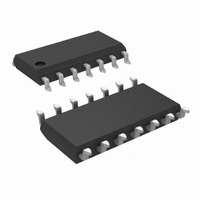
IC OPAMP TFT-LCD QUAD 16V 14SOIC
Manufacturer
National Semiconductor
Series
VIP10™r
Datasheet
1.LM6588MANOPB.pdf
(16 pages)
Specifications of LM6588MAX/NOPB
Applications
TFT-LCD Panels: Gamma Buffer, VCOM Driver
Output Type
Rail-to-Rail
Number Of Circuits
4
-3db Bandwidth
24MHz
Slew Rate
15 V/µs
Current - Supply
800µA
Current - Output / Channel
230mA
Voltage - Supply, Single/dual (±)
5 V ~ 16 V, ±2.5 V ~ 8 V
Mounting Type
Surface Mount
Package / Case
14-SOIC (0.154", 3.90mm Width)
Number Of Channels
4
Voltage Gain Db
106 dB
Common Mode Rejection Ratio (min)
70 dB
Input Offset Voltage
4 mV at 5 V
Operating Supply Voltage
9 V, 12 V, 15 V
Supply Current
4 mA at 5 V
Maximum Operating Temperature
+ 85 C
Maximum Dual Supply Voltage
+/- 8 V
Minimum Operating Temperature
- 40 C
Lead Free Status / RoHS Status
Lead free / RoHS Compliant
Other names
LM6588MAX
Available stocks
Company
Part Number
Manufacturer
Quantity
Price
Company:

Part Number:
LM6588MAX/NOPB
Manufacturer:
NS/TI
Quantity:
2 200


www.national.com
TFT Display Application
8KHz to 160KHz, which is much lower than the gain band-
width of most op amps. As a result, the V
little phase lag when op amp loop gain is unity, and this
allows the V
measuring the small-signal bandwidth of the LM6588 with
the RC load of Figure 4. When driving an RC load of 50nF
and 20Ω, the LM6588 has a unity gain frequency of 6.12MHz
with 41.5˚C of phase margin. If the load capacitor is in-
creased to 200nF and the resistance remains 20Ω, the unity
gain frequency is virtually unchanged: 6.05MHz with 42.9˚C
of phase margin.
A V
the op amp’s maximum output current, not by its slew rate.
This is easily shown by calculating how much output current
is required to slew a 50nF load capacitance at the LM6588
slew rate of 14V/µs:
700mA exceeds the maximum current specification for the
LM6588 and almost all other op amps, confirming that a
V
order to minimize V
V
COM
COM
COM
FIGURE 4. V
driver’s speed is limited by its peak output current. In
Driver must supply large values of output current.
Driver’s large-signal response time is determined by
FIGURE 5. V
COM
Driver to remain stable. This was verified by
I
COM
OUT
COM
= 14V/µs x 50nF
Driver with Simplified Load
COM
= 700mA
transients, the op amp used as a
Driver Test Circuit
COM
(Continued)
load adds very
20073430
20073429
12
Figure 5 is a common test circuit used for measuring V
driver response time. The RC network of R
to C
network is a gross simplification of what the actual imped-
ance is on a TFT panel. However, it does provide a useful
test for measuring the op amp’s transient response when
driving a large capacitive load. A low impedance MOSFET
driver applies a 5V square wave to V
current pulses in the RC network. Scope photos from this
circuit are shown in Figure 6 and Figure 7. Figure 6 shows
the test circuit generates positive and negative voltage
spikes with an amplitude of
both transients settle-out in approximately 2µs. As men-
tioned before, the speed at which these transients settle-out
is a function of the op amp’s peak output current. The I
trace in Figure 7 shows that the LM6588 can sink and source
peak currents of −200mA and 200mA. This ability to supply
large values of output current makes the LM6588 extremely
well suited for V
FIGURE 7. V
FIGURE 6. V
4
models the distributed RC load of a V
SW
COM
SW
and I
and V
Driver applications.
OUT
Circuit
COM
Waveforms from V
±
3.2V at the V
Waveforms from V
SW
, generating large
COM
L1
COM
20073431
20073432
to R
line. This RC
COM
node, and
L3
COM
and C
Test
COM
OUT
1
Related parts for LM6588MAX/NOPB
Image
Part Number
Description
Manufacturer
Datasheet
Request
R

Part Number:
Description:
Op Amps
Manufacturer:
National Semiconductor
Datasheet:

Part Number:
Description:
IC OPAMP TFT-LCD QUAD 16V 14SOIC
Manufacturer:
National Semiconductor
Datasheet:
Part Number:
Description:
Op Amps
Manufacturer:
National Semiconductor
Datasheet:
Part Number:
Description:
National Semiconductor [8-Bit D/A Converter]
Manufacturer:
National Semiconductor
Datasheet:
Part Number:
Description:
National Semiconductor [Media Coprocessor]
Manufacturer:
National Semiconductor
Datasheet:
Part Number:
Description:
Digitally Controlled Tone and Volume Circuit with Stereo Audio Power Amplifier, Microphone Preamp Stage and National 3D Sound
Manufacturer:
National Semiconductor
Datasheet:
Part Number:
Description:
Digitally Controlled Tone and Volume Circuit with Stereo Audio Power Amplifier, Microphone Preamp Stage and National 3D Sound
Manufacturer:
National Semiconductor
Datasheet:
Part Number:
Description:
AC97 Rev 2 Codec with Sample Rate Conversion and National 3D Sound
Manufacturer:
National Semiconductor
Part Number:
Description:
Manufacturer:
National Semiconductor
Datasheet:
Part Number:
Description:
Manufacturer:
National Semiconductor
Datasheet:
Part Number:
Description:
General Purpose, Low Voltage, Low Power, Rail-to-Rail Output Operational Amplifiers
Manufacturer:
National Semiconductor
Datasheet:
Part Number:
Description:
8-bit 20 MSPS flash A/D converter.
Manufacturer:
National Semiconductor
Datasheet:
Part Number:
Description:
Low Noise Quad Operational Amplifier
Manufacturer:
National Semiconductor
Datasheet:
Part Number:
Description:
Quad Differential Line Receivers
Manufacturer:
National Semiconductor
Datasheet: