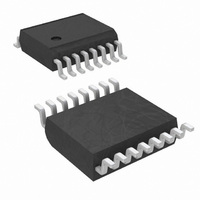
LMH6739MQ/NOPB National Semiconductor, LMH6739MQ/NOPB Datasheet - Page 8

LMH6739MQ/NOPB
Manufacturer Part Number
LMH6739MQ/NOPB
Description
IC VIDEO BUFFER TRPL PROG 16SSOP
Manufacturer
National Semiconductor
Datasheet
1.LMH6739MQXNOPB.pdf
(12 pages)
Specifications of LMH6739MQ/NOPB
Applications
Buffer
Number Of Circuits
3
-3db Bandwidth
750MHz
Slew Rate
3300 V/µs
Current - Supply
32mA
Current - Output / Channel
90mA
Voltage - Supply, Single/dual (±)
8 V ~ 12 V, ±4 V ~ 6 V
Mounting Type
Surface Mount
Package / Case
16-LSSOP (0.154", 3.91mm Width)
No. Of Amplifiers
3
Gain Bandwidth
750MHz
Supply Voltage Range
8V To 12V
Output Current
90mA
Amplifier Output
Single Ended
Operating Temperature Range
-40°C To +85°C
Rohs Compliant
Yes
For Use With
LMH730275 - EVAL BOARD HS TRIPLE SSOP OPAMP
Lead Free Status / RoHS Status
Lead free / RoHS Compliant
Other names
*LMH6739MQ
*LMH6739MQ/NOPB
LMH6739MQ
*LMH6739MQ/NOPB
LMH6739MQ
www.national.com
Application Information
FIGURE 1. Recommended Non-Inverting Gain Circuit,
FIGURE 2. Recommended Non-Inverting Gain Circuit,
FIGURE 3. Recommended Inverting Gain Circuit,
Gain = +2
Gain = –1
Gain +1
20104105
20104103
20104108
8
GENERAL INFORMATION
The LMH6739 is a high speed current feedback selectable
gain buffer (SGB), optimized for very high speed and low dis-
tortion. With its internal feedback and gain-setting resistors
the LMH6739 offers excellent AC performance while simpli-
fying board layout and minimizing the affects of layout related
parasitic components. The LMH6739 has no internal ground
reference so single or split supply configurations are both
equally useful.
SETTING THE CLOSED LOOP GAIN
The LMH6739 is a current feedback amplifier with on-chip
R
A
as described in the chart below.
The gain of the LMH6739 is accurate to ±1% and stable over
temperature. The internal gain setting resistors, R
match very well. However, over process and temperature
their absolute value will change. Using external resistors in
series with R
curacy over temperature and from part to part.
−1 V/V
+1 V/V
+2 V/V
FIGURE 5. Frequency Response for Circuit in Figure 4
V
F
= +2, A
= R
GAIN A
FIGURE 4. Correction for Unity Gain Peaking
G
= 450Ω. As such it can be configured with an
V
V
= +1, or an A
G
to change the gain will result in poor gain ac-
Non-Inverting
Ground
Input Signal
Input Signal
V
INPUT CONNECTIONS
= −1 by connecting pins 3 and 4
Inverting
Input Signal
NC (Open)
Ground
20104129
F
and R
20104130
G
,


