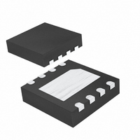
MAX9509ATA+T Maxim Integrated Products, MAX9509ATA+T Datasheet - Page 2

MAX9509ATA+T
Manufacturer Part Number
MAX9509ATA+T
Description
IC AMP VIDEO FILTER 8-TDFN
Manufacturer
Maxim Integrated Products
Series
DirectDrive™r
Datasheet
1.MAX9509ATAT.pdf
(17 pages)
Specifications of MAX9509ATA+T
Applications
Filter
Number Of Circuits
1
-3db Bandwidth
42.1MHz
Slew Rate
43 V/µs
Current - Supply
3.1mA
Current - Output / Channel
82mA
Voltage - Supply, Single/dual (±)
1.7 V ~ 2.63 V
Mounting Type
Surface Mount
Package / Case
8-TDFN Exposed Pad
Number Of Channels
1
Supply Current
3.1 mA
Minimum Operating Temperature
- 40 C
Maximum Operating Temperature
+ 125 C
Bandwidth
42.1 MHz
Maximum Power Dissipation
953.5 mW
Mounting Style
SMD/SMT
Supply Voltage (max)
2.625 V
Supply Voltage (min)
1.7 V
Lead Free Status / RoHS Status
Lead free / RoHS Compliant
ABSOLUTE MAXIMUM RATINGS
(Voltages with respect to GND.)
V
IN ................................................................-0.3V to (V
OUT .......................(The greater of V
SHDN........................................................................-0.3V to +4V
C1P ............................................................-0.3V to (V
C1N ............................................................(V
V
Duration of OUT Short Circuit to V
1.8V, Ultra-Low Power, DirectDrive
Video Filter Amplifiers
ELECTRICAL CHARACTERISTICS
(V
noted. Typical values are at T
Stresses beyond those listed under “Absolute Maximum Ratings” may cause permanent damage to the device. These are stress ratings only, and functional
operation of the device at these or any other conditions beyond those indicated in the operational sections of the specifications is not implied. Exposure to
absolute maximum rating conditions for extended periods may affect device reliability.
2
Supply Voltage Range
Supply Current
Shutdown Supply Current
Output Level
DC-COUPLED INPUT
Input Voltage Range
Input Current
Input Resistance
AC-COUPLED INPUT
Sync-Tip Clamp Level
Input-Voltage Swing
Sync Crush
Input Clamping Current
Line Time Distortion
Minimum Input Source
Resistance
DD
SS
GND, and V
DD
...........................................................................-3V to +0.3V
_______________________________________________________________________________________
..........................................................................-0.3V to +3V
= SHDN = 1.8V, GND = 0V, OUT has R
PARAMETER
SS
.........................................................Continuous
A
= +25°C.) (Note 1)
SYMBOL
I
DD
V
SHDN
V
I
R
DD
CLP
I
DD
B
IN
SS
,
and -1V) to (V
Guaranteed by PSRR
No load
SHDN = GND
IN = 80mV
Guaranteed by output
voltage swing
IN = 130mV
10mV
C
Guaranteed by output
voltage swing
Percentage reduction in sync pulse at output,
R
IN = 130mV
C
SS
SOURCE
IN
IN
L
- 0.3V) to +0.3V
= 0.1µF
= 0.1µF
= 150Ω connected to GND, C1 = C2 = 1µF, T
IN
DD
DD
DD
= 37.5 , C
+ 0.3V)
+ 0.3V)
+ 0.3V)
250mV
CONDITIONS
IN
= 0.1µF
MAX9509
MAX9510
1.7V
2.375V
Continuous Current
Continuous Power Dissipation (T
Operating Temperature Range ........................-40°C to +125°C
Junction Temperature .....................................................+150°C
Storage Temperature Range .............................-65°C to +150°C
Lead Temperature (soldering, 10s) .................................+300°C
1.7V
2.375V
IN, SHDN .......................................................................±20mA
8-Pin TDFN (derate 11.9mW/°C above +70°C) .........953.5mW
8-Pin µMAX (derate 4.5mW/°C above +70°C) ..............362mW
V
V
DD
DD
V
V
DD
DD
2.625V
2.625V
2.625V
2.625V
1.700
A
MIN
-75
-8
= T
0
0
A
MIN
= +70°C)
TYP
0.01
to T
280
3.1
2.9
1.6
0.2
+5
25
2
0
2
MAX
, unless otherwise
2.625
262.5
252.5
MAX
+75
+11
325
325
5.3
4.9
3.2
3.2
10
UNITS
mV
mA
mV
mV
mV
k
µA
µA
µA
%
%
V
P-P


