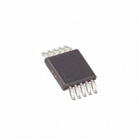
MAX9585AUB+ Maxim Integrated Products, MAX9585AUB+ Datasheet - Page 2

MAX9585AUB+
Manufacturer Part Number
MAX9585AUB+
Description
IC AMP VIDEO FILTER 10-UMAX
Manufacturer
Maxim Integrated Products
Datasheet
1.MAX9583AZTT.pdf
(15 pages)
Specifications of MAX9585AUB+
Applications
Filter
Number Of Circuits
4
Current - Supply
3.5mA
Current - Output / Channel
140mA
Voltage - Supply, Single/dual (±)
2.7 V ~ 3.6 V
Mounting Type
Surface Mount
Package / Case
10-MSOP, Micro10™, 10-uMAX, 10-uSOP
Number Of Channels
4
Supply Current
3.5 mA
Minimum Operating Temperature
- 40 C
Maximum Operating Temperature
+ 125 C
Maximum Power Dissipation
444 mW
Mounting Style
SMD/SMT
Supply Voltage (max)
3.6 V
Supply Voltage (min)
2.7 V
Lead Free Status / RoHS Status
Lead free / RoHS Compliant
ABSOLUTE MAXIMUM RATINGS
V
IN_ to GND ...............................................................-0.3V to +4V
OUT_ Short-Circuit Duration to V
Continuous Input Current
Continuous Power Dissipation (T
Dual, Triple, and Quad Standard-Definition Video
Filter Amplifiers with DC-Coupled Input Buffers
Stresses beyond those listed under “Absolute Maximum Ratings” may cause permanent damage to the device. These are stress ratings only, and functional
operation of the device at these or any other conditions beyond those indicated in the operational sections of the specifications is not implied. Exposure to
absolute maximum rating conditions for extended periods may affect device reliability.
ELECTRICAL CHARACTERISTICS
(V
2
Supply Voltage Range
Supply Current
Input Voltage Range
Input Current
Input Resistance
DC Voltage Gain (Note 2)
DC Gain Matching
Output Level
Output-Voltage Swing
Output Short-Circuit
Current
Output Resistance
Power-Supply Rejection
Ratio
DD
DD
IN_ ................................................................................±20mA
6-Pin Thin SOT23 (derate 9.1mW/°C above +70°C) ....727mW
_______________________________________________________________________________________
to GND ..............................................................-0.3V to +4V
= 3.3V, GND = 0V, R
PARAMETER
L
= no load, T
SYMBOL
PSRR
R
V
I
V
R
DD
A
I
Av
OUT
DD
DD
IN
IN
IN
= +70°C)
, GND .................Continuous
A
Guaranteed by PSRR
Per channel
Guaranteed by DC
voltage gain
V
R
Guaranteed by DC voltage gain
Measured at V
Measured at output, V
R
Measured at output, V
R
Measured at output, V
R
Measured at output, V
R
M easur ed at outp ut, V
R
Short to GND (sourcing)
Short to V
V
2.7V
f = 1MHz, 100mV
= T
IN
L
OUT
L
L
L
L
L
= 150 to GND
= 150 to -0.2V
= 150 to V
= 150 to -0.2V
= 150 to V
= 75 to - 0.2V
= 0V
MIN
= 1.5V, -10mA
V
DD
to T
DD
MAX
(sinking)
3.6V
OUT
DD
DD
, unless otherwise noted. Typical values are at T
P-P
/2
/2
, V
CONDITIONS
IN
D D
DD
DD
DD
DD
I
= 0V, R
LOAD
= 3.135V , 0V
= 2.7V, 0V
= 2.7V, 0V
= 3V, 0V
= 3V, 0V
V
0V
V
0V
Operating Temperature Range .........................-40°C to +125°C
Junction Temperature ......................................................+150°C
Storage Temperature Range .............................-65°C to +150°C
Lead Temperature (soldering, 10s) .................................+300°C
DD
DD
L
10mA
8-Pin µMAX (derate 4.5mW/°C above +70°C) .............362mW
10-Pin µMAX (derate 5.6mW/°C above +70°C) ...........444mW
V
V
= 2.7V,
= 3V,
V
V
= 150 to GND
DD
DD
IN
IN
= 2.7V
= 3V
V
V
IN
IN
1.05V
1.2V
V
V
IN
IN
V
I N
1. 2V,
1. 2V,
1.05V,
1.05V,
1.05V ,
0.210
1.92
1.92
MIN
2.7
48
-2
0
0
A
0.300
TYP
140
= +25°C) (Note 1)
3.5
0.6
2.1
2.1
2.4
2.4
2.1
0.2
25
70
29
2
2
0
0.410
MAX
1.05
2.04
2.04
3.6
1.2
10
+2
7
UNITS
V
V
M
mA
V/V
mA
dB
µA
%
P-P
P-P
V
V


