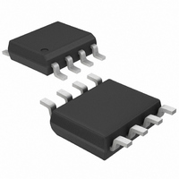
MAX4310ESA+T Maxim Integrated Products, MAX4310ESA+T Datasheet - Page 2

MAX4310ESA+T
Manufacturer Part Number
MAX4310ESA+T
Description
IC AMP VIDEO MUX 8-SOIC
Manufacturer
Maxim Integrated Products
Datasheet
1.MAX4310ESA.pdf
(18 pages)
Specifications of MAX4310ESA+T
Applications
2:1 Multiplexer-Amplifier
Output Type
Rail-to-Rail
Number Of Circuits
1
-3db Bandwidth
280MHz
Slew Rate
460 V/µs
Current - Supply
6.1mA
Current - Output / Channel
95mA
Voltage - Supply, Single/dual (±)
4 V ~ 10.5 V, ±2 V ~ 5.25 V
Mounting Type
Surface Mount
Package / Case
8-SOIC (0.154", 3.90mm Width)
Lead Free Status / RoHS Status
Lead free / RoHS Compliant
High-Speed, Low-Power, Single-Supply
Multichannel, Video Multiplexer-Amplifiers
ABSOLUTE MAXIMUM RATINGS
Supply Voltage (V
Input Voltage....................................(V
All Other Pins ...................................(V
Output Current................................................................±120mA
Short-Circuit Duration (V
Continuous Power Dissipation (T
DC ELECTRICAL CHARACTERISTICS
(V
Stresses beyond those listed under “Absolute Maximum Ratings” may cause permanent damage to the device. These are stress ratings only, and functional
operation of the device at these or any other conditions beyond those indicated in the operational sections of the specifications is not implied. Exposure to
absolute maximum rating conditions for extended periods may affect device reliability.
2
8-Pin SO (derate 5.9mW/°C above +70°C)...................471mW
8-Pin µMAX (derate 4.1mW/°C above +70°C) ..............330mW
CC
Operating Supply Voltage
Range
Input Voltage Range
Common-Mode Rejection
Ratio
Input Offset Voltage
Input Offset Voltage Drift
Input Offset Voltage
Matching
Input Bias Current
Feedback Bias Current
Input Offset Current
Common-Mode Input
Resistance
Differential Input Resistance
Output Resistance
Disabled Output Resistance
Open-Loop Gain
Voltage Gain
_______________________________________________________________________________________
= +5V, V
PARAMETER
EE
= 0V, SHDN ≥ 4V, R
CC
to V
OUT
EE
) .................................................12V
to GND, V
A
SYMBOL
= +70°C)
TC
CMRR
L
R
R
A
A
V
V
I
R
R
I
= ∞, V
OUT
OUT
VOL
EE
I
OS
VCL
FB
EE
CC
OS
VOS
B
IN
IN
CC
- 0.3V) to (V
- 0.3V) to (V
or V
OUT
EE
Inferred from PSRR test
MAX4310/MAX4311/MAX4312, inferred from
CMRR test
MAX4313/MAX4314/MAX4315, inferred from
output voltage swing
0 ≤ V
only
I
I
MAX4310/MAX4311/MAX4312 only
V
MAX4312 only
MAX4310/MAX4311/
MAX4312 only
MAX4313/MAX4314/MAX4315
MAX4310/MAX4311/MAX4312, open loop
MAX4313/MAX4314/MAX4315
MAX4310/MAX4311/MAX4312,
R
MAX4313/MAX4314/MAX4315,
R
IN
FB
= 2.5V, T
IN
L
L
)....Continuous
, MAX4310/MAX4311/MAX4312 only
= 150Ω to GND, 0.25V ≤ V
= 150Ω to GND, 0.25V ≤ V
varied over V
CM
CC
CC
+ 0.3V)
+ 0.3V)
≤ 2.2V, MAX4310/MAX4311/MAX4312
A
= T
MIN
CONDITIONS
CM
to T
, MAX4310/MAX4311/
MAX
Operating Temperature Range ...........................-40°C to +85°C
Storage Temperature Range .............................-65°C to +150°C
Lead Temperature (soldering, 10s) .................................+300°C
Open loop
Closed loop, A
14-Pin SO (derate 8.3mW/°C above +70°C).................667mW
16-Pin SO (derate 8.7mW/°C above +70°C).................696mW
16-Pin QSOP (derate 8.3mW/°C above +70°C)............667mW
, unless otherwise noted. Typical values are at T
OUT
OUT
≤ 4.2V
≤ 4.2V
V
= +1V/V
0.035
0.035
MIN
4.0
1.9
73
50
0.025
0.025
TYP
±5.0
0.1
2.0
±7
±1
95
70
35
59
7
7
3
8
1
V
V
CC
CC
MAX
- 2.8
- 2.7
10.5
±20
2.1
14
14
2
A
= +25°C.)
UNITS
µV/°C
MΩ
mV
mV
KΩ
V/V
dB
µA
µA
µA
dB
Ω
Ω
V
V


