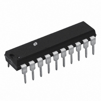
LM1279AN National Semiconductor, LM1279AN Datasheet - Page 9

LM1279AN
Manufacturer Part Number
LM1279AN
Description
IC AMP RGB VIDEO SYSTEM 20-DIP
Manufacturer
National Semiconductor
Datasheet
1.LM1279AN.pdf
(14 pages)
Specifications of LM1279AN
Applications
General Purpose
Number Of Circuits
3
-3db Bandwidth
110MHz
Current - Supply
80mA
Current - Output / Channel
28mA
Voltage - Supply, Single/dual (±)
7.5 V ~ 8.5 V
Mounting Type
Through Hole
Package / Case
20-DIP (0.300", 7.62mm)
Lead Free Status / RoHS Status
Contains lead / RoHS non-compliant
Other names
*LM1279AN
Available stocks
Company
Part Number
Manufacturer
Quantity
Price
Company:
Part Number:
LM1279AN
Manufacturer:
NSC
Quantity:
5 510
Company:
Part Number:
LM1279AN
Manufacturer:
PHI
Quantity:
5 510
Part Number:
LM1279AN
Manufacturer:
NS/国半
Quantity:
20 000
Applications of the LM1279
age surges that may result during the power up and power
down modes, or when connecting the monitor to other equip-
ment. The monitor designer must include these resistors in
his design for good monitor reliability. If additional protection
against ESD at the video inputs is necessary, then adding
clamp diodes on the IC side of the 30
mended, one to V
Sometimes a designer may want to increase the value of the
30
tion. This is not recommended with the LM1279. C5, C7, and
C9 are part of the DC restoration circuit. This circuit is de-
pending on a total maximum circuit resistance of about
110 ; 30 input series resistor plus 75 for the video termi-
nation resistor. Increasing the value of the 30
exceed the 110 limit. The excellent internal ESD protection
and the external clamp diodes (if needed) will provide excel-
lent ESD protection.
The 30
necessary if the OSD signals are external to the monitor, or
if these signals are present any time when the +8V is not
fully powered up. Interfacing to the OSD inputs is quite easy
since the signal processing necessary to match the OSD sig-
nals to the video levels is done internal by the LM1279.
There is also no need for an OSD window signal. Any time
there is a high TTL signal at any of the three OSD inputs, the
LM1279 will automatically switch to the OSD mode. A high
TTL OSD signal will give a high video output for that color.
The OSD level is fixed, typically 2.3V above the video black
level. This will give a fixed brightness to the OSD window,
but not at maximum video brightness which could be un-
pleasant to the user. Figure 2 and Figure 3 show the timing
diagrams of the OSD signals for the LM1279.
The recommended load impedance for the LM1279 is 390 .
However, some changes in the load impedance can be
made. If the load impedance is reduced, the monitor de-
signer must confirm that the part is still operating in its proper
die temperature range, never exceeding a die temperature
resistors at the video inputs, for additional ESD protec-
resistors in series with the OSD inputs are also
CC1
and one to ground (see Figure 6 ).
resistors is recom-
(Continued)
resistors will
9
of 150˚C. When changing the load impedance, the black
level shift is shown in the chart below. The measured V
output with under 1% distortion is also listed.
When using a lower load impedance, the LM1279 does go
into hard clipping more quickly. This does reduce the head-
room of the video output.
Board layout is always critical in a high frequency application
such as using the LM1279. A poor layout can result in ringing
of the video waveform after sudden transitions, or the part
could actually oscillate. A good ground plane and proper
routing of the +8V are important steps to a good PCB layout.
The LM1279 does require very good coupling between V
and V
and Figure 11 with the short and large trace between pins 2
and 16. Both demonstration boards offer the monitor de-
signer an excellent example of good ground plane being
used with the LM1279. These boards are single sided, yet al-
low the LM1279 to operate at its peak performance. The
neck board also shows a good example of interfacing to a
CRT driver and to the CRT. The video signal path is kept as
short as possible between the LM1279 and the CRT driver,
and also between the CRT driver and the CRT socket. Actual
performance of the LM1279 in the video pre-amp demon-
stration board is shown in Figure 8 and Figure 9 .
References
Ott, Henry W. Noise Reduction Techniques in Electronic
Systems , John Wiley & Sons, New York, 1976
Zahid Rahim, “Guide to CRT Video Design,” Application
Note 861, National Semiconductor Corp., Jan. 1993
430
390
330
270
Load
CC2
(pins 2 and 16). This is clearly shown in Figure 7
3.62V
3.62V
3.58V
3.51V
V
P-P
Blk. Level Shift
+15 mV
−25 mV
−45 mV
0 mV
www.national.com
CC1
P-P


