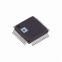
ADAU1701JSTZ Analog Devices Inc, ADAU1701JSTZ Datasheet - Page 10

ADAU1701JSTZ
Manufacturer Part Number
ADAU1701JSTZ
Description
IC AUDIO PROC 2ADC/4DAC 48-LQFP
Manufacturer
Analog Devices Inc
Series
SigmaDSP®r
Type
Audio Processorr
Specifications of ADAU1701JSTZ
Design Resources
Analog Audio Input, Class-D Output with ADAU1701, SSM2306, and ADP3336 (CN0162)
Applications
Automotive, Monitors, MP3
Mounting Type
Surface Mount
Package / Case
48-LQFP
Audio Control Type
Digital
Control Interface
I2C, Serial
Supply Voltage Range
1.8V, 3.3V
Operating Temperature Range
0°C To +70°C
Audio Ic Case Style
LQFP
No. Of Pins
48
Svhc
No SVHC
Control / Process Application
MP3 Player Speaker Docks, Automotive Head Units, Studio Monitors
Rohs Compliant
Yes
Lead Free Status / RoHS Status
Lead free / RoHS Compliant
For Use With
EVAL-ADAU1701MINIZ - BOARD EVAL SIGMADSP AUD ADAU1701EVAL-ADAU1701EBZ - BOARD EVAL FOR ADAU1701
Lead Free Status / RoHS Status
Lead free / RoHS Compliant, Lead free / RoHS Compliant
Available stocks
Company
Part Number
Manufacturer
Quantity
Price
Company:
Part Number:
ADAU1701JSTZ
Manufacturer:
Analog Devices Inc
Quantity:
1 923
Company:
Part Number:
ADAU1701JSTZ
Manufacturer:
ADI
Quantity:
221
Company:
Part Number:
ADAU1701JSTZ
Manufacturer:
Analog Devices Inc
Quantity:
10 000
Part Number:
ADAU1701JSTZ
Manufacturer:
ADI/亚德诺
Quantity:
20 000
Company:
Part Number:
ADAU1701JSTZ-RL
Manufacturer:
ON
Quantity:
35 000
Company:
Part Number:
ADAU1701JSTZ-RL
Manufacturer:
Analog Devices Inc
Quantity:
10 000
Part Number:
ADAU1701JSTZ-RL
Manufacturer:
ADI/亚德诺
Quantity:
20 000
ADAU1701
Pin No.
14
15
16
17
18
19
20
21
22
23
26
27
28
29
30
31
32
33
34
35
36, 48
Mnemonic
MP7
MP6
MP10
VDRIVE
IOVDD
MP11
ADDR1/CDATA/WB
CLATCH/WP
SDA/COUT
SCL/CCLK
MP9
MP8
MP3
MP2
RSVD
OSCO
MCLKI
PGND
PVDD
PLL_LF
AVDD
Type
D_IO
D_IO
D_IO
A_OUT
PWR
D_IO
D_IN
D_IO
D_IO
D_IO
D_IO/A_IO
D_IO/A_IO
D_IO/A_IO
D_IO/A_IO
X
D_OUT
D_IN
PWR
PWR
A_OUT
PWR
1
Page No.
43
43
43
4
43
21, 23, 25
23, 25
20, 23
20, 23
43
43
43
43
16
16
16
Rev. 0 | Page 10 of 52
Description
Multipurpose GPIO or Serial Output Port Data 1 (SDATA_OUT1).
Multipurpose GPIO, Serial Output Port Data 0, or TDM Data Output
(SDATA_OUT0).
Multipurpose GPIO or Serial Output Port LRCLK (OUTPUT_LRCLK).
Drive for 1.8 V Regulator. The base of the voltage regulator external PNP
transistor is driven from VDRIVE.
Supply for Input and Output Pins. The voltage on this pin sets the highest
input voltage that should be seen on the digital input pins. This pin is also
the supply for the digital output signals on the control port and MP pins.
IOVDD should always be set to 3.3 V. The current draw of this pin is variable
because it is dependent on the loads of the digital outputs.
Multipurpose GPIO or Serial Output Port BCLK (OUTPUT_BCLK).
ADDR1: I
of the IC so that four ADAU1701s can be used on the same I
CDATA: SPI Data Input.
WB: EEPROM Writeback Trigger. A rising (default) or falling (if set in the
EEPROM messages) edge on this pin triggers a writeback of the interface
registers to the external EEPROM. This function can be used to save
parameter data on power-down.
CLATCH: SPI Latch Signal. Must go low at the beginning of an SPI transaction
and high at the end of a transaction. Each SPI transaction can take a different
number of CCLKs to complete, depending on the address and read/write bit
that are sent at the beginning of the SPI transaction.
WP: Self-Boot EEPROM Write Protect. This pin is an open-collector output
when in self-boot mode. The ADAU1701 pulls this low to prohibit writes to
an external EEPROM. This pin should be pulled high to 3.3 V.
SDA: I
to this pin should have a 2.2 kΩ pull-up resistor.
COUT: This SPI data output is used for reading back registers and memory
locations. It is three-stated when an SPI read is not active.
SCL: I
mode. In self-boot mode, this pin is an open-collector output (I
The line connected to this pin should have a 2.2 kΩ pull-up resistor.
CCLK: SPI Clock. This pin can either run continuously or be gated off in
between SPI transactions.
Multipurpose GPIO, Serial Output Port Data 3 (SDATA_OUT3), or Auxiliary
ADC Input 0.
Multipurpose GPIO, Serial Output Port Data 2 (SDATA_OUT2), or Auxiliary
ADC Input 3.
Multipurpose GPIO, Serial Input Port Data 3 (SDATA_IN3), or Auxiliary
ADC Input 2.
Multipurpose GPIO, Serial Input Port Data 2 (SDATA_IN2), or Auxiliary
ADC Input 1.
Reserved. Tie to ground, either directly or through a pull-down resistor.
Crystal Oscillator Circuit Output. A 100 Ω damping resistor should be
connected between this pin and the crystal. This output should not be used
to directly drive a clock to another IC. If the crystal oscillator is not used, this
pin can be left disconnected.
Master Clock Input. MCLKI can either be connected to a 3.3 V clock signal or
can be the input from the crystal oscillator circuit.
PLL Ground Pin. The AGND, DGND, and PGND pins can be tied directly
together in a common ground plane. PGND should be decoupled to PVDD
with a 100 nF capacitor.
3.3 V Power Supply for the PLL and the Auxiliary ADC Analog Section. This
should be decoupled to PGND with a 100 nF capacitor.
PLL Loop Filter Connection. Two capacitors and a resistor need to be connected
to this pin, as shown in the Setting Master Clock/PLL Mode section.
3.3 V Analog Supply. This should be decoupled to AGND with a 100 nF capacitor.
2
2
C Clock. This pin is always an open-collector input when in I
C Data. This pin is a bidirectional open-collector. The line connected
2
C Address 1. In combination with ADDR0, this sets the I
2
C bus.
2
C master).
2
C address
2
C control


