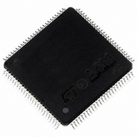
TDA7500A STMicroelectronics, TDA7500A Datasheet - Page 6

TDA7500A
Manufacturer Part Number
TDA7500A
Description
IC PROCESSOR AM/FM DGTL 100-TQFP
Manufacturer
STMicroelectronics
Type
Audio Processorr
Datasheet
1.TDA7500ATR.pdf
(40 pages)
Specifications of TDA7500A
Applications
Audio Systems
Mounting Type
Surface Mount
Package / Case
100-TQFP Exposed Pad, 100-eTQFP, 100-HTQFP, 100-VQFP
Lead Free Status / RoHS Status
Lead free / RoHS Compliant
Available stocks
Company
Part Number
Manufacturer
Quantity
Price
Company:
Part Number:
TDA7500ATR
Manufacturer:
STMicroelectronics
Quantity:
10 000
Part Number:
TDA7500ATR
Manufacturer:
ST
Quantity:
20 000
TDA7500A
PIN DESCRIPTION (continued)
6/40
N°
46
47
48
49
50
51
52
53
54
55
56
57
58
59
SRA<9>
SRA<10>
SRA<11>
SRA<12>
CGND2
CVDD2
SRA<13>
SRA<14>
SRA<15>
SRA<16>/DSP0_GPIO8
DWR
DRD
CASALE
SDO<2>/SRA<17>/DSP1_GPIO<8>
Name
Type
O
O
O
O
O
O
O
O
O
O
O
O
Line<9> (Output). This pin acts as the EMI address line 9 in both
SRAM Mode and DRAM Mode
Line<10> (Output). This pin acts as the EMI address line 10 in
both SRAM Mode and DRAM Mode
Line<11> (Output). This pin acts as the EMI address line 11 in
both SRAM Mode and DRAM Mode
Line<12> (Output). This pin acts as the EMI address line 12 in
both SRAM Mode and DRAM Mode
Ground pin dedicated to the digital circuitry.
Supply pin dedicated to the digital circuitry.
Line<13> (Output). This pin act as the EMI address line 13 in
both SRAM Mode and DRAM Mode.
Line<14> (Output). This pin act as the EMI address line 14 in
both SRAM Mode and DRAM Mode.
Line<15> (Output). This pin act as the EMI address line 15 in
both SRAM Mode and DRAM Mode.
Line<16> (Output)/General Purpose I/O (Input/Output). This pin
acts as the EMI address line 16 in both SRAM Mode and DRAM
Mode. Optionally it can be used as general purpose I/O
controlled by DSP0. After reset the state of this pin is read by the
boot SW to select the boot mode (Refer to HW/SW maual).
DSP SRAM Write Enable (Output)/DRAM Write Enable
(Output). This pin serves as the write enable for the EMI in both
DRAM and SRAM Mode (active low). To be connected to R/W of
the RAM.
DSP SRAM Read Enable(Output)/DRAM Read Enable (Output).
This pin serves as the read enable for the EMI in both DRAM
and SRAM Mode (active low). To be connected to R/W of the
RAM.
Mode this pin acts as the column address strobe.
SAI Outputs (Output)/EMI SRAM Address Line<17> (Output)/
General Purpose I/O (Input/Output). One stereo channel SAI
data output in SAI mode. EMI address line 17 in SRAM Mode.
Optionally it can be used as a general purpose I/O.
DSP SRAM Address Line<9> (Output)/DSP DRAM Address
DSP SRAM Address Line<10> (Output)/DSP DRAM Address
DSP SRAM Address Line<11> (Output)/DSP DRAM Address
DSP SRAM Address Line<12> (Output)/DSP DRAM Address
DSP SRAM Address Line<13> (Output)/DSP DRAM Address
DSP SRAM Address Line<14> (Output)/DSP DRAM Address
DSP SRAM Address Line<15> (Output)/DSP DRAM Address
DSP SRAM Address Line<16> (Output)/DSP DRAM Address
DSP DRAM Column Address Strobe (Output). When in DRAM
Description


