CLC5903SM/NOPB National Semiconductor, CLC5903SM/NOPB Datasheet
CLC5903SM/NOPB
Specifications of CLC5903SM/NOPB
*CLC5903SM/NOPB
CLC5903SM
Available stocks


Related parts for CLC5903SM/NOPB

CLC5903SM/NOPB Summary of contents
Page 1
... IF A DVGA IF B DVGA LC CLK Figure 1. Diversity Receiver Chipset Block Diagram ©2004 National Semiconductor Corporation Features 78MSPS Operation Low Power, 145mW/channel, 52 MHz, Dec=192 Two Independent Channels with 14-bit inputs Serial Daisy-chain Mode for quad receivers Greater than 100 dB image rejection Greater than 100 dB spurious free dynamic range ...
Page 2
RD Microprocessor WR Interface CE A[7:0] D[7:0] AIN MUX BIN A MUX B TEST_REG Input Source A_SOURCE B_SOURCE CKA CLK GEN CKB SI Sync MR Logic Figure 2. CLC5903 Dual Digital Tuner / AGC Block Diagram with Control Register Associations ...
Page 3
Absolute Maximum Ratings Positive IO Supply Voltage (V ) DDIO Positive CoreSupply Voltage ( Voltage on Any Input or Output Pin Input Current at Any Pin Package Input Current Package Dissipation at T =25°C A ESD Susceptibility Human ...
Page 4
AC Characteristics (Continued) (F =78MHz, CIC Decimation=48, F2 Decimation=2; unless specified) S Parameter (C Symbol t MR Setup Time to CKA|B (Figure 5) MRSU t MR Hold Time to CKA|B (Figure 5) MRH t SI Setup Time to CKA|B (Figure ...
Page 5
AC Characteristics (Continued) (F =78MHz, CIC Decimation=48, F2 Decimation=2; unless specified) S Parameter (C Symbol t Controlling strobe pulse width (Write) (Figure 15) CSPW t Control output delay controlling signal low to D (Read) (Figure 15) CDLY t Control tri-state ...
Page 6
CLC5903VLA Pinout VDDIO 39 BGAIN[2] 40 BGAIN[1] 41 BGAIN[0] 42 BSTROBE VSSIO A[7] 48 VDD 49 50 A[6] VSS 51 A[ A[3] A[ A[1] A[0] 57 ...
Page 7
Pin Descriptions (Continued) Signal PQFP Pin FBGA Pin AOUT 82 G12 BOUT 78 G10 AGAIN[2:0], 125:127 D4,A3,D5 BGAIN[2:0] 40:42 J5,L4,M3 ASTROBE, 124 C4 BSTROBE 43 K5 SCK 80 H11 SCK_IN 99 B11 SFS 81 F9 F12,F10, 84,86:88, E11,E12, 90,91, D11,D12, ...
Page 8
Pin Descriptions (Continued) Signal PQFP Pin FBGA Pin J9,L10, 62,63, M12,K11, D[7:0] 69:73,75 L12,H9, J11,H10 M5,L6,L7, 48,50, A[7:0] K7,L8,M8, 52:57 K8, TDO 116 B6 TDI 117 C6 TMS 118 B5 TCK ...
Page 9
Timing Diagrams Figure 6. CLC5903 Synchronization Input (SI) Timing t CKDC CKA|B A|BIN Figure 7. CLC5903 ADC Input and Clock Timing t CKL CKA CKB CK A|BSTROBE A|BGAIN[2..0] t MRH t MRSU t ...
Page 10
Timing Diagrams (Continued) SCK SCK_POL=0 SCK SCK_POL=1 t SFSV SFS SFS_POL=0 SFS SFS_POL=1 A|BOUT Previous Q Output Word RDY RDY_POL=0 RDY RDY_POL=1 t RDYV POUT_EN t OENV POUT[15..0] POUT_SEL[2.. SELV POUT[15..0] output (n) RDY RDY_POL=0 RDY RDY_POL=1 t ...
Page 11
TCK t JPCO t JPEN TDO TCK TDI, TDS TCK t JSCO t JSEN D TCK D Figure 14. CLC5903 JTAG Port Timing CSU A[7:0] D[7: CSU A[7:0] D[7: ...
Page 12
Detailed Description (Continued) Detailed Description Control Interface The CLC5903 is configured by writing control information into 148 control registers within the chip. The contents of these control registers and how to use them are described under Control Register Addresses and ...
Page 13
Detailed Description (Continued) the compensation is dependent on timing and the accuracy of the DVGA gain step. The CLC5903 allows the timing of the gain compensation to be adjusted in the EXT_DELAY regis- ter. This operating mode requires 21 bits ...
Page 14
Detailed Description (Continued) The 2’s complement format represents full-scale negative as 10000000 and full-scale positive as 01111111 for an 8-bit example. The 16 bit phase offset is set by loading the PHASE register according to the formula PHASE = 2 ...
Page 15
Detailed Description (Continued) mum headroom through the CIC filter. For optimal noise per- formance the SCALE value is set to increase this level until the CIC filter is just below the point of distortion. A value is normally calculated and ...
Page 16
Detailed Description (Continued) Frequency Response of F2 Using STD Set 0 −10 −20 −30 −40 −50 −60 −70 −80 −90 −100 0 0.1 0.2 Frequency Normalized To Filter Input Sample Rate Figure 23. F2 STD frequency response Frequency Response of ...
Page 17
Output Modes (Continued) Combined Frequency Response of CIC/F1/F2 Using GSM Set 1 0.5 0 −0.5 −1 −1.5 − Frequency (KHz) Figure 28. CIC, F1, & F2 GSM Passband Flatness decreases relative to the output sample rate, ...
Page 18
Output Modes (Continued) SCK SFS AOUT (a) UNPACKED MODE, FRAME SYNC AT THE START OF EACH WORD SCK SFS AOUT (b) PACKED MODE, ONE FRAME SYNC AT THE START OF EACH DOUBLE-WORD TRANSFER leading edge of RDY aligns with leading ...
Page 19
AGC (Continued) Slave CLC5903 SDC_EN=0 MUX_MODE=0 PACKED=1 ADCs and DVGAs chip sends the I data first by setting SFS high (or low if SFS_POL in the input control register is set high) for one clock cycle, and then transmitting the ...
Page 20
Test and Diagnostics level. DVGA operation results in a compression of the signal through the ADC. The DVGA signal compression is reversed in the CLC5903 to provide > 120dB of linear dynamic range. This is illustrated in Figure 32. Diversity ...
Page 21
SCK will be set to the proper strobe rate for each debug tap point. POUT_EN and PSEL[2..0] have no effect in Debug Mode. The outputs are turned on when the Debug Mode bit is set. Normal serial outputs are also ...
Page 22
Control Register Addresses and Defaults Register Name Width Type Default AGC_IC_B 1B R/W AGC_RB_A 1B R AGC_RB_B 1B R TEST_REG 14b R/W Reserved 1B - Reserved 1B - DEBUG_EN 1b R/W DEBUG_TAP 5b R/W DITH_A 1b R/W DITH_B 1b R/W ...
Page 23
Condensed CLC5903 Address Map Addr Register Name Addr Hex DEC_BY_4 1 0x01 SCALE 2 0x02 GAIN_A 3 0x03 GAIN_B 4 0x04 RATE 5 0x05 SERIAL_CTRL 6 0x06 FREQ_A 7 0x07 8 0x08 9 0x09 10 0x0A PHASE_A 11 0x0B 12 ...
Page 24
AGC Theory of Operation AGC Theory of Operation A block diagram of the AGC is shown in Figure 34. The DVGA interface comprises four pins for each of the channels. The first three pins of this interface are a 3-bit ...
Page 25
AGC Theory of Operation leading ‘1’ out of the CIC filter. An output of ‘001XX’ corre- sponds to a leading ‘1’ in bit 2 (LSB is bit 0). The exponent increases by one each time the leading ‘1’ advances in ...
Page 26
AGAIN EXP Input 000 = -12dB 111 = +0dB -12dB 001 = -6dB 110 = -6dB -12dB 010 = +0dB 101 = -12dB -12dB 011 = +6dB 100 ...
Page 27
Evaluation Hardware Evaluation boards are available to facilitate designs based on the CLC5903: CLC-EDRCS-PCASM The Enhanced Diversity Receiver Chipset evaluation board providing a complete narrowband receiver from IF to digital symbols. CLC-CAPT-PCASM A simple method for capturing output data from ...
Page 28
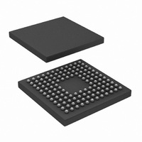
Physical Dimensions CLC5903SM www.national.com inches (millimeters) unless otherwise noted. Figure 39. CLC5903SM FBGA Package Dimensions 28 ...
Page 29
... NATIONAL’S PRODUCTS ARE NOT AUTHORIZED FOR USE AS CRITICAL COMPONENTS IN LIFE SUPPORT DEVICES OR SYSTEMS WITHOUT THE EXPRESS WRITTEN APPROVAL OF THE PRESIDENT AND GEN- ERAL COUNSEL OF NATIONAL SEMICONDUCTOR CORPORATION. As used herein: 1. Life support devices or systems are devices or sys- tems which, (a) are intended for surgical implant ...