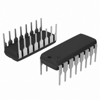
SA572NG ON Semiconductor, SA572NG Datasheet - Page 4

SA572NG
Manufacturer Part Number
SA572NG
Description
IC COMPANDOR 2CHAN GAIN 16-DIP
Manufacturer
ON Semiconductor
Type
Compandorr
Datasheet
1.SA572DTBR2.pdf
(12 pages)
Specifications of SA572NG
Applications
Automatic Level Control, Stereo Expander
Mounting Type
Through Hole
Package / Case
16-DIP (0.300", 7.62mm)
Maximum Operating Temperature
+ 85 C
Mounting Style
Through Hole
Minimum Operating Temperature
- 40 C
Lead Free Status / RoHS Status
Lead free / RoHS Compliant
Other names
SA572NG
SA572NGOS
SA572NGOS
Available stocks
Company
Part Number
Manufacturer
Quantity
Price
Part Number:
SA572NG
Manufacturer:
ON/安森美
Quantity:
20 000
Audio Signal Processing IC Combines VCA and
Fast Attack/Slow Recovery Level Sensor
is desirable to independently control the attack and
recovery time of the gain control signal. This is true, for
example, in compandor applications for noise reduction. In
high end systems the input signal is usually split into two
or more frequency bands to optimize the dynamic behavior
for each band. This reduces low frequency distortion due
to control signal ripple, phase distortion, high frequency
channel overload and noise modulation. Because of the
expense in hardware, multiple band signal processing up to
now was limited to professional audio applications.
performance noise reduction concept becomes feasible for
consumer hi fi applications. The SA572 is a dual channel
gain control IC. Each channel has a linearized,
temperature-compensated gain cell and an improved level
sensor. In conjunction with an external low noise op amp
for current-to-voltage conversion, the VCA features low
distortion, low noise and wide dynamic range.
Description
compensated gain cells (DG), each with a full-wave
rectifier and a buffer amplifier as shown in the block
diagram. The two channels share a 2.5 V common bias
reference derived from the power supply but otherwise
operate independently. Because of inherent low distortion,
low noise and the capability to linearize large signals, a
wide dynamic range can be obtained. The buffer amplifiers
are provided to permit control of attack time and recovery
time independent of each other. Partitioned as shown in the
block diagram, the IC allows flexibility in the design of
system levels that optimize DC shift, ripple distortion,
tracking accuracy and noise floor for a wide range of
application requirements.
Gain Cell
Bases of the differential pairs Q
tied to the output and inputs of OPA A
feedback through Q
of Q
from the transistor model equation in the forward active
region.
In high-performance audio gain control applications, it
With the introduction of the SA572 this high-
The SA572 consists of two linearized, temperature-
Figure 3 shows the circuit configuration of the gain cell.
3
-Q
4
equal. The following relationship can be derived
DV
(V
1
BE
holds the V
BE
Q3Q4
= V
T
+ D
I
IN
IC/IS)
1
BE
BE
-Q
Q1Q2
of Q
2
and Q
1
-Q
1
. The negative
2
3
-Q
and the V
BASIC APPLICATIONS
4
are both
http://onsemi.com
BE
4
current for the VCA gives lower gain control ripple and
independent control of fast attack, slow recovery dynamic
response. An attack capacitor C
resistor R
t
an internal 10 kW resistor R
for the high-frequency spectrum and 40 ms for the low
frequency band can be obtained with 0.1 mF and 1.0 mF
attack capacitors, respectively. Recovery time of 200 ms
can be obtained with a 4.7 mF recovery capacitor for a
100 Hz signal, the third harmonic distortion is improved by
more than 10 dB over the simple RC ripple filter with a
single 1.0 mF attack and recovery capacitor, while the
attack time remains the same.
plastic package and in oversized SOL package. It operates
over a wide supply range from 6.0 V to 22 V. Supply
current is less than 6.0 mA. The SA572 is designed for
applications from −40°C to +85°C.
where I
is the gain control current of the gain cell.
equation 1 can be simplified to:
relationship of a linearized two quadrant transconductance
amplifier. The second term is the gain control feedthrough
due to the mismatch of devices. In the design, this has been
minimized by large matched devices and careful layout.
Offset voltage is caused by the device mismatch and it leads
to even harmonic distortion. The offset voltage can be
trimmed out by feeding a current source within "25 mA
into the THD trim pin.
R
The novel level sensor which provides gain control
The SA572 is assembled in a standard 16-pin dual in-line
R
I
I
I
If all transistors Q
The first term of equation 2 shows the multiplier
1
2
of a tone burst is defined by a recovery capacitor C
O
1
= 140 mA
= 280 mA
is the differential output current of the gain cell and I
= 6.8 kW
IN
V
+ V
I
A
+
O
T
I
defines the attack time t
n
+ 2
T
V
R
I
n
IN
1
2
1
I
I
2
G
I
@ I
1
)
I
S
) I
I
S
IN
1
2
1
I
IN
O
through Q
@ I
* V
* V
G
R
. Typical attack time of 4.0 ms
* 1
T
T
I
I
A
n
I
n
2
4
with an internal 10 kW
I
I
2
2
are of the same size,
1
2
A
* 2I
* I
I
. The recovery time
G
* 1
I
1
I
S
S
1
2
* I
I
@ I
O
IN
G
(eq. 1)
R
(eq. 2)
and
G


