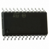
TDA7476 STMicroelectronics, TDA7476 Datasheet - Page 10

TDA7476
Manufacturer Part Number
TDA7476
Description
IC PROCESSOR RADIO DIAGN 24-SOIC
Manufacturer
STMicroelectronics
Type
Car Signal Processorr
Datasheet
1.E-TDA7476013TR.pdf
(19 pages)
Specifications of TDA7476
Applications
Automotive Systems
Mounting Type
Surface Mount
Package / Case
24-SOIC (7.5mm Width)
Lead Free Status / RoHS Status
Lead free / RoHS Compliant
Available stocks
Company
Part Number
Manufacturer
Quantity
Price
Part Number:
TDA7476
Manufacturer:
ST
Quantity:
20 000
Company:
Part Number:
TDA7476013TR
Manufacturer:
MICREL
Quantity:
6 350
Part Number:
TDA7476013TR
Manufacturer:
ST
Quantity:
20 000
Part Number:
TDA7476TR
Manufacturer:
ST
Quantity:
20 000
Company:
Part Number:
TDA7476TR-7LF
Manufacturer:
WDC
Quantity:
165
Part Number:
TDA7476TR-7LF
Manufacturer:
ST
Quantity:
20 000
TDA7476
I
Data transmission from microprocessor to the TDA7476 and viceversa takes place through the 2 wires I
interface, consisting of the two lines SDA and SCL (pull-up resistors to positive supply voltage must be connected).
Data Validity
As shown by fig. 2, the data on the SDA line must be stable during the high period of the clock. The HIGH and
LOW state of the data line can only change when the clock signal on the SCL line is LOW.
Start and Stop Conditions
As shown by fig. 3 a start condition is a HIGH to LOW transition of the SDA line while SCL is HIGH. The stop
condition is a LOW to HIGH transition of the SDA line while SCL is HIGH.
Byte Format
Every byte transferred to the SDA line must contain 8 bits. Each byte must be followed by an acknowledge bit.
The MSB is transferred first.
Acknowledge
The transmitter* puts a resistive HIGH level on the SDA line during the acknowledge clock pulse (see fig.4). The
receiver** the acknowledges has to pull-down (LOW) the SDA line during the acknowledge clock pulse, so that
the SDAline is stable LOW during this clock pulse.
* Transmitter
** Receiver
Figure 2. Data Validity on the I
10/19
2
C BUS INTERFACE
The minimum voltage of the AUX IN pins to sense the open load condition is 2V.
The minimum voltage of the AUX IN pin to detect the short circuit to GND by sensing drop on the resistor
is 4.5V. If this voltage is below 2V, the AUX line is considered short circuited to GND. From 2V to 4.5V
the sensing circuit can detect a short circuit in both ways (by sensing across the resistor or through the
voltage between the AUX IN pin and GND).
= master ( P) when it writes an address to the TDA7476
= slave (TDA7476) when the P reads a data byte from TDA7476
= slave (TDA7476) when the P writes an address to the TDA7476
= master ( P) when it reads a data byte from TDA7476
SDA
SCL
STABLE, DATA
DATA LINE
2
CBUS
VALID
ALLOWED
CHANGE
DATA
D99AU1031
2
C BUS


