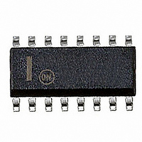
NE570D ON Semiconductor, NE570D Datasheet - Page 8

NE570D
Manufacturer Part Number
NE570D
Description
IC COMPANDOR DUAL GAIN 16-SOIC
Manufacturer
ON Semiconductor
Type
Compandorr
Datasheet
1.NE570DR2G.pdf
(10 pages)
Specifications of NE570D
Applications
Cellular Radio, Players
Mounting Type
Surface Mount
Package / Case
16-SOIC (0.300", 7.5mm Width)
Lead Free Status / RoHS Status
Contains lead / RoHS non-compliant
Available stocks
Company
Part Number
Manufacturer
Quantity
Price
Part Number:
NE570D
Manufacturer:
NXP/恩智浦
Quantity:
20 000
Part Number:
NE570DG
Manufacturer:
ON/安森美
Quantity:
20 000
Part Number:
NE570DR2G
Manufacturer:
ON/安森美
Quantity:
20 000
this, which means our overall offsets are typically about mV.
The distortion is not affected by the magnitude of the gain
control current, and it does not increase as the gain is
changed. This second harmonic distortion could be
eliminated by making perfect transistors, but since that
would be difficult, we have had to resort to other methods.
A trim pin has been provided to allow trimming of the
internal offsets to zero, which effectively eliminated second
harmonic distortion. Figure 14 shows the simple trim
network required.
maximum output level before clipping occurs in the gain cell
is plotted along with the output noise in a 20 kHz bandwidth.
Note that the noise drops as the gain is reduced for the first
20 dB of gain reduction. At high gains, the signal to noise
ratio is 90 dB, and the total dynamic range from maximum
signal to minimum noise is 110 dB.
Figure 15 shows the noise performance of the DG cell. The
−100
+20
−20
−40
−60
−80
0
−40
Figure 14. THD Trim Network
To THD Trim
Figure 15. Dynamic Range
110 dB
200 pF
VCA GAIN (dB)
−20
6.2 kW
SIGNAL LEVEL
MAXIMUM
V
CC
3.6 V
R
20 kW
0
20 kHz BW
NOISE IN
90 dB
http://onsemi.com
NE570
8
imperfect device matching and mismatches in the current
sources, I
I
effective in nulling out any control signal feedthrough, but
in general, the null for minimum feedthrough will be
different than the null in distortion. The control signal
feedthrough can be trimmed independently of distortion by
tying a current source to the DG input pin. This effectively
trims I
OPERATIONAL AMPLIFIER
equivalent to a 741 with a 1.0 MHz bandwidth. Figure 17
shows the basic circuit. Split collectors are used in the input
pair to reduce g
just 10 pF may be used. The output stage, although capable
of output currents in excess of 20 mA, is biased for a low
quiescent current to conserve power. When driving heavy
loads, this leads to a small amount of crossover distortion.
G
Control signal feedthrough is generated in the gain cell by
The main op amp shown in the chip block diagram is
will cause a small output signal. The distortion trim is
1
−IN
. Figure 16 shows such a trim network.
Figure 16. Control Signal Feedthrough
1
and I
Figure 17. Operational Amplifier
Q
100 kW
3
Q
M
2
1
. When no input signal is present, changing
, so that a small compensation capacitor of
Q
V
I
2
CC
1
Q
3.6 V
R−SELECT FOR
4
+IN
C
470 kW
C
Q
5
D
D
I
2
1
2
TO PIN 3 OR 14
Q
6
OUT


