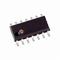
MCP6544-E/SL Microchip Technology, MCP6544-E/SL Datasheet - Page 3

MCP6544-E/SL
Manufacturer Part Number
MCP6544-E/SL
Description
IC COMP 1.6V QUAD P-P 14SOIC
Manufacturer
Microchip Technology
Type
General Purposer
Specifications of MCP6544-E/SL
Output Type
CMOS, Push-Pull, Rail-to-Rail, TTL
Package / Case
14-SOIC (0.154", 3.90mm Width)
Number Of Elements
4
Voltage - Supply
1.6 V ~ 5.5 V
Mounting Type
Surface Mount
Number Of Channels
4 Channels
Product
Analog Comparators
Offset Voltage (max)
7 mV
Input Bias Current (max)
0.000001 uA
Supply Voltage (max)
5.5 V
Supply Voltage (min)
1.6 V
Maximum Operating Temperature
+ 125 C
Mounting Style
SMD/SMT
Minimum Operating Temperature
- 40 C
Lead Free Status / RoHS Status
Lead free / RoHS Compliant
DC CHARACTERISTICS (CONTINUED)
AC CHARACTERISTICS
MCP6543 CHIP SELECT (CS) CHARACTERISTICS
© 2006 Microchip Technology Inc.
Electrical Specifications: Unless otherwise indicated, V
V
Push-Pull Output
High-Level Output Voltage
Low-Level Output Voltage
Short-Circuit Current
Note 1:
Electrical Specifications: Unless otherwise indicated, V
Step = 200 mV, Overdrive = 100 mV, and C
Rise Time
Fall Time
Propagation Delay (High-to-Low)
Propagation Delay (Low-to-High)
Propagation Delay Skew
Maximum Toggle Frequency
Input Noise Voltage
Note 1:
Electrical Specifications: Unless otherwise indicated, V
and C
CS Low Specifications
CS Logic Threshold, Low
CS Input Current, Low
CS High Specifications
CS Logic Threshold, High
CS Input Current, High
CS Input High, V
CS Input High, GND Current
Comparator Output Leakage
CS Dynamic Specifications
CS Low to Comparator Output Low
Turn-on Time
CS High to Comparator Output
High Z Turn-off Time
CS Hysteresis
IN –
= V
L
2:
3:
4:
= 36 pF (Refer to Figures 1-1 and 1-3).
SS
Parameters
Parameters
Parameters
, and R
The input offset voltage is the center (average) of the input-referred trip points. The input hysteresis is the difference
between the input-referred trip points.
V
Input bias current at temperature is not tested for SC-70-5 package.
Limit the output current to Absolute Maximum Rating of 30 mA.
Propagation Delay Skew is defined as: t
HYST
DD
at different temperatures is estimated using V
Current
L
= 100 kΩ to V
V
DD
I
CS_HYST
O(LEAK)
Sym
Sym
I
t
f
f
I
t
t
t
V
t
MAX
MAX
V
CSH
I
I
OFF
Sym
PDS
E
CSL
/2 (Refer to
PHL
PLH
DD
ON
V
t
SS
V
t
R
IH
I
I
F
IL
ni
OH
SC
SC
OL
L
= 36 pF (Refer to
0.8 V
Min
Min
V
V
—
—
—
—
—
—
—
—
—
—
—
—
—
—
—
—
PDS
SS
DD
Min
DD
Figure
—
—
—
−0.2
= t
DD
DD
PLH
= +1.6V to +5.5V, V
Typ
0.85
0.85
±0.2
= +1.6V to +5.5V, V
Typ
–20
160
120
200
5.0
0.6
18
10
—
—
1
1
2
4
4
1-3).
-2.5, +1.5
Figure 1-2
- t
DD
HYST
Typ
±30
PHL
—
—
= +1.6V to +5.5V, V
0.2 V
.
MCP6541/1R/1U/2/3/4
Max
(T
Max
V
50
—
—
—
—
—
—
—
—
—
—
—
—
—
DD
8
8
A
) = V
and
DD
V
SS
Max
—
—
—
Figure
HYST
+0.2
Units
Units
µV
SS
kHz
kHz
SS
ms
pA
pA
pA
pA
pA
µs
µs
µs
µs
µs
µs
V
V
V
P-P
= GND, T
= GND, T
+ (T
1-3).
Units
(Note 1)
V
V
10 Hz to 100 kHz
CS = V
CS = V
CS = V
CS = V
V
CS = 0.2 V
V
CS = 0.8 V
V
V
mA
mA
A
V
V
DD
DD
OUT
IN
IN
DD
SS
- 25°C) TC
– = V
– = V
= 1.6V
= 5.5V
= 5V
A
A
= GND, T
= V
= +25°C, V
I
I
V
V
= +25°C, V
SS
DD
DD
DD
OUT
OUT
DD
DD
DD
DD
DD
DD
DD
= 1.6V (Note 4)
= 5.5V (Note 4)
, CS = V
= -2 mA, V
= 2 mA, V
1
to V
to V
+ (T
Conditions
Conditions
A
= +25°C,V
IN
OUT
OUT
IN
A
Conditions
+ = V
+ = V
- 25°C)
DD
= V
= V
DD
DD
DD
DD
DS21696E-page 3
DD
DD
= 5V
= 5V
2
/2,
/2, V
/2,
/2,
TC
IN
+ = V
2
IN
.
–
= V
DD
SS
/2,
,


