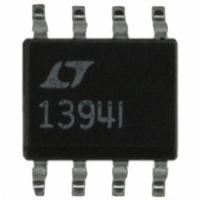
LT1394IS8#PBF Linear Technology, LT1394IS8#PBF Datasheet - Page 6

LT1394IS8#PBF
Manufacturer Part Number
LT1394IS8#PBF
Description
IC COMPARATOR LOW PWR 7NS 8-SOIC
Manufacturer
Linear Technology
Series
UltraFast™r
Type
General Purposer
Datasheet
1.LT1394CS8PBF.pdf
(16 pages)
Specifications of LT1394IS8#PBF
Number Of Elements
1
Output Type
CMOS, Complementary, TTL
Mounting Type
Surface Mount
Package / Case
8-SOIC (0.154", 3.90mm Width)
Comparator Type
General Purpose
No. Of Comparators
1
Response Time
7ns
Ic Output Type
CMOS, MOS, Open-Collector / Drain, TTL
Supply Current
6mA
Rohs Compliant
Yes
Number Of Elements
1
Input Offset Voltage
2.5mV
Input Bias Current (typ)
4.5uA
Supply Current (max)
8.5@±5VmA
Power Supply Requirement
Single/Dual
Common Mode Rejection Ratio
100dB
Voltage Gain In Db
64.08dB
Power Supply Rejection Ratio
100dB
Single Supply Voltage (max)
12V
Dual Supply Voltage (max)
±6V
Operating Temp Range
-40C to 85C
Operating Temperature Classification
Industrial
Mounting
Surface Mount
Pin Count
8
Package Type
SOIC N
Lead Free Status / RoHS Status
Lead free / RoHS Compliant
Available stocks
Company
Part Number
Manufacturer
Quantity
Price
PIN
LT1394
TYPICAL PERFORMANCE CHARACTERISTICS
V
+IN (Pin 2): Noninverting Input.
–IN (Pin 3): Inverting Input.
V
– 5V.
LATCH ENABLE (Pin 5): Latch Control Pin. When high, the
outputs remain in a latched condition, independent of the
current state of the inputs.
6
TI I G DIAGRA S
V
OUT
V
+
–
IN
U
(Pin 4): Negative Supply Voltage. Normally either 0V or
W
(Pin 1): Positive Supply Voltage. Normally 5V.
FUNCTIONS
U
+ IN
U
–95mV
V
IN
5mV
t
5mV Overdrive
V
f
V
PD
IN
V
S
OD
OD
= 5V
= 2MHz
+
= 5mV
U
Response Time to
W
W
t
PD
2ns/DIV
U
1394 TD01
1394 G17
1.4V
Q OUT
0V
ENABLE
LATCH
V
OUT
V
IN
GND (Pin 6): Ground.
Q OUT (Pin 7): Noninverting Logic Output. This pin is high
when +IN is above –IN and LATCH ENABLE is low.
Q OUT (Pin 8): Inverting Logic Output. This pin is low
when +IN is above –IN and LATCH ENABLE is low.
+ IN
–95mV
5mV
V
f
V
t
5mV Overdrive
IN
t
PD
S
OD
SU
= 5V
= 2MHz
= 5mV
–
Response Time to
t
2ns/DIV
H
1394 G18
t
1.4V
0V
Q OUT
L PD
1394 TD02


