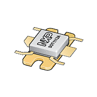
BLF6G27L-50BN NXP Semiconductors, BLF6G27L-50BN Datasheet - Page 4

BLF6G27L-50BN
Manufacturer Part Number
BLF6G27L-50BN
Description
50 W LDMOS power transistor for base station applications at frequencies from 2500 MHz to 2700 MHz
Manufacturer
NXP Semiconductors
Datasheet
1.BLF6G27L-50BN.pdf
(16 pages)
NXP Semiconductors
BLF6G27L-50BN_6G27LS-50BN
Product data sheet
Fig 1.
(dB)
G
(1) f = 2500 MHz
(2) f = 2600 MHz
(3) f = 2700 MHz
17.0
16.5
16.0
15.5
15.0
14.5
p
0
V
Single carrier IS-95 power gain as a function of
load power; typical values
DS
= 28 V; I
7.1 Ruggedness in Class-AB operation
7.2 Single carrier IS-95
5
Dq
= 430 mA.
Table 8.
All testing performed in Class-AB production test circuit; test signal 3GPP; test model 1; 64 DPCH;
PAR = 7.2 dB at 0.01 % probability on CCDF per carrier; f = 2700 MHz; RF performance at
V
The BLF6G27L-50BN and BLF6G27LS-50BN are capable of withstanding a load
mismatch corresponding to VSWR = 10 : 1 through all phases under the following
conditions: V
Single carrier IS-95 with pilot, paging, sync and 6 traffic channels (Walsh codes 8 - 13).
PAR = 9.7 dB at 0.01 % probability on the CCDF. Channel bandwidth is 1.2288 MHz.
Symbol
PAR
10
DS
= 28 V; I
O
15
1-carrier W-CDMA application information
Parameter
output peak-to-average ratio
Dq
DS
(1)
(2)
(3)
= 430 mA; T
20
All information provided in this document is subject to legal disclaimers.
= 28 V; I
001aan474
P
L
(W)
25
Dq
Rev. 2 — 7 April 2011
case
= 430 mA; P
= 25
°
C; unless otherwise specified.
Fig 2.
(%)
(1) f = 2500 MHz
(2) f = 2600 MHz
(3) f = 2700 MHz
L
D
50
40
30
20
10
= 40 W (CW); f = 2500 MHz.
0
0
V
Single carrier IS-95 drain efficiency as a
function of load power; typical values
DS
Conditions
P
L(AV)
= 28 V; I
BLF6G27L(S)-50BN
5
= 16 W
Dq
= 430 mA.
10
Min
4.1
Power LDMOS transistor
15
Typ
4.7
© NXP B.V. 2011. All rights reserved.
20
001aan478
(1)
(2)
(3)
P
L
(W)
Max
5.3
25
Unit
dB
4 of 16


