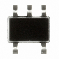
TS3021ICT STMicroelectronics, TS3021ICT Datasheet - Page 2

TS3021ICT
Manufacturer Part Number
TS3021ICT
Description
IC COMP R-R 1.8V HS SC70-5
Manufacturer
STMicroelectronics
Type
General Purposer
Datasheet
1.TS3021ICT.pdf
(16 pages)
Specifications of TS3021ICT
Number Of Elements
1
Output Type
Push-Pull
Voltage - Supply
1.8 V ~ 5 V
Mounting Type
Surface Mount
Package / Case
6-TSSOP (5 lead), SC-88A, SOT-353
Number Of Channels
1 Channel
Response Time
0.048 us
Offset Voltage (max)
8 mV
Input Bias Current (max)
0.16 uA
Supply Voltage (max)
5 V
Supply Voltage (min)
2 V
Supply Current (max)
0.115 mA
Maximum Power Dissipation
600 mW
Maximum Operating Temperature
+ 125 C
Mounting Style
SMD/SMT
Minimum Operating Temperature
- 40 C
Number Of Elements
1
Technology
BiCMOS
Input Offset Voltage
6mV
Input Bias Current (typ)
160nA
Single Supply Voltage (typ)
3V
Dual Supply Voltage (typ)
Not RequiredV
Power Supply Requirement
Single
Common Mode Rejection Ratio
79dB
Power Supply Rejection Ratio
69dB
Single Supply Voltage (min)
2V
Single Supply Voltage (max)
5V
Dual Supply Voltage (min)
Not RequiredV
Dual Supply Voltage (max)
Not RequiredV
Power Dissipation
600mW
Operating Temp Range
-40C to 125C
Operating Temperature Classification
Automotive
Mounting
Surface Mount
Pin Count
5
Package Type
SC-70
Lead Free Status / RoHS Status
Lead free / RoHS Compliant
Other names
497-5324-2
Available stocks
Company
Part Number
Manufacturer
Quantity
Price
Company:
Part Number:
TS3021ICT
Manufacturer:
STMicroelectronics
Quantity:
2 400
Part Number:
TS3021ICT
Manufacturer:
ST
Quantity:
20 000
Absolute maximum ratings and operating conditions
1
2/16
Absolute maximum ratings and operating conditions
Table 1.
1. All voltage values, except differential voltage, are referenced to V
2. The magnitude of input and output voltages must never exceed the supply rail ±0.3 V.
3. Short-circuits can cause excessive heating. These values are typical.
4. Human body model: a 100 pF capacitor is charged to the specified voltage, then discharged through a
5. Machine model: a 200 pF capacitor is charged to the specified voltage, then discharged directly between
6. Charged device model: all pins and the package are charged together to the specified voltage and then
Table 2.
Symbol
Symbol
1.5 kΩ resistor between two pins of the device. This is done for all couples of connected pin combinations
while the other pins are floating.
two pins of the device with no external series resistor (internal resistor < 5 Ω). This is done for all couples of
connected pin combinations while the other pins are floating.
discharged directly to the ground through only one pin. This is done for all pins.
T
V
V
T
oper
R
R
ESD
V
icm
T
CC
LEAD
V
V
T
thja
CC
thjc
stg
ID
IN
j
Operating temperature range
Supply voltage
Common mode input voltage range
Absolute maximum ratings
Operating conditions
0°C < T
-40°C < T
-40°C < T
+85°C < T
Supply voltage
Differential input voltage
Input voltage range
Thermal resistance junction to ambient
Thermal resistance junction to case
Storage temperature
Junction temperature
Lead temperature (soldering 10 seconds)
Human body model (HBM)
Machine model (MM)
Charged device model (CDM)
Latch-up immunity
SC70-5
SOT23-5
SC70-5
SOT23-5
amb
amb
amb
amb
< +125°C
< +125°C
< +85°C
< +125°C
(1)
Parameter
Parameter
(5)
(2)
(4)
(6)
(3)
(3)
DD
.
V
DD
-0.3 to V
-65 to +150
V
Value
5000
1500
150
260
DD
205
250
172
300
200
5.5
±5
81
-40 to +125
-0.2 to V
V
DD
1.8 to 5
CC
Value
2 to 5
+0.3
to V
CC
CC
+0.2
TS3021
°C/W
°C/W
Unit
mA
°C
°C
°C
Unit
V
V
V
V
°C
V
V


