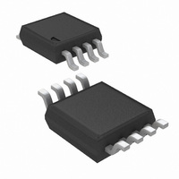
LMV393MMX/NOPB National Semiconductor, LMV393MMX/NOPB Datasheet - Page 10

LMV393MMX/NOPB
Manufacturer Part Number
LMV393MMX/NOPB
Description
IC COMP TINY DUAL LOW V 8-MSOP
Manufacturer
National Semiconductor
Type
General Purposer
Datasheet
1.LMV331M5XNOPB.pdf
(20 pages)
Specifications of LMV393MMX/NOPB
Number Of Elements
2
Output Type
CMOS, Open-Collector, TTL
Voltage - Supply
2.7 V ~ 5.5 V
Mounting Type
Surface Mount
Package / Case
8-TSSOP, 8-MSOP (0.118", 3.00mm Width)
Leaded Process Compatible
Yes
Rohs Compliant
Yes
Peak Reflow Compatible (260 C)
Yes
Lead Free Status / RoHS Status
Lead free / RoHS Compliant
Other names
LMV393MMX
LMV393MMXTR
LMV393MMXTR
Available stocks
Company
Part Number
Manufacturer
Quantity
Price
Company:
Part Number:
LMV393MMX/NOPB
Manufacturer:
IDT
Quantity:
6 246
Part Number:
LMV393MMX/NOPB
Manufacturer:
TI/德州仪器
Quantity:
20 000
www.national.com
PULSE GENERATOR WITH VARIABLE DUTY CYCLE
The pulse generator with variable duty cycle is just a minor
modification of the basic square wave generator. Providing a
separate charge and discharge path for capacitor C
ates a variable duty cycle. One path, through R
charge the capacitor and set the pulse width (t
path, R
between pulses (t
By varying resistor R
erator can be changed without changing the pulse width.
Similarly, by varying R
affecting the time between pulses. Both controls will change
the frequency of the generator. The pulse width and time be-
tween pulses can be found from:
1
and D
FIGURE 6. Crystal controlled Oscillator
1
FIGURE 7. Pulse Generator
will discharge the capacitor and set the time
2
).
1
2
, the time between pulses of the gen-
, the pulse width will be altered without
1
2
). The other
and D
10008009
10008007
1
gener-
2
will
10
Solving these equations for t
These terms will have a slight error due to the fact that V
is not exactly equal to 2/3 V
diode drop to:
POSITIVE PEAK DETECTOR
Positive peak detector is basically the comparator operated
as a unit gain follower with a large holding capacitor from the
output to ground. Additional transistor is added to the output
to provide a low impedance current source. When the output
of the comparator goes high, current is passed through the
transistor to charge up the capacitor. The only discharge path
will be the 1 MΩ resistor shunting C1 and any load that is
connected to the output. The decay time can be altered simply
by changing the 1 MΩ resistor. The output should be used
through a high impedance follower to a avoid loading the out-
put of the peak detector.
t
t
1
2
=R
=R
CC
1
4
5
and t
C
C
but is actually reduced by the
1
1
ln2
ln2
2
max


