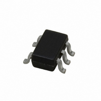
LPV7215MG/NOPB National Semiconductor, LPV7215MG/NOPB Datasheet - Page 13

LPV7215MG/NOPB
Manufacturer Part Number
LPV7215MG/NOPB
Description
IC COMP 1.8V P-P R-R I/O SC70-5
Manufacturer
National Semiconductor
Series
PowerWise®r
Type
General Purposer
Datasheet
1.LPV7215MFNOPB.pdf
(18 pages)
Specifications of LPV7215MG/NOPB
Number Of Elements
1
Output Type
MOS, Push-Pull, Rail-to-Rail
Voltage - Supply
1.8 V ~ 5.5 V
Mounting Type
Surface Mount
Package / Case
6-TSSOP (5 lead), SC-88A, SOT-353
Comparator Type
General Purpose
No. Of Comparators
1
Response Time
4.5µs
Ic Output Type
Push Pull
Supply Current
580nA
Supply Voltage Range
1.8V To 5.5V
Amplifier Case Style
SC-70
Rohs Compliant
Yes
Number Of Elements
1
Technology
CMOS
Input Offset Voltage
3mV
Single Supply Voltage (typ)
3/5V
Dual Supply Voltage (typ)
Not RequiredV
Supply Current (max)
0.00103@5VmA
Power Supply Requirement
Single
Common Mode Rejection Ratio
98dB
Voltage Gain In Db
120dB
Power Supply Rejection Ratio
82dB
Single Supply Voltage (min)
1.8V
Single Supply Voltage (max)
5.5V
Dual Supply Voltage (min)
Not RequiredV
Dual Supply Voltage (max)
Not RequiredV
Operating Temp Range
-40C to 85C
Operating Temperature Classification
Industrial
Mounting
Surface Mount
Pin Count
5
Package Type
SC-70
Lead Free Status / RoHS Status
Lead free / RoHS Compliant
Other names
LPV7215MG
LPV7215MGTR
LPV7215MGTR
Available stocks
Company
Part Number
Manufacturer
Quantity
Price
CAPACITIVE AND RESISTIVE LOADS
The propagation delay is not affected by capacitive loads at
the output of the LPV7215. However, resistive loads slightly
affect the propagation delay on the falling edge by a reduction
of almost 2 µs depending on the load resistance value.
NOISE
Most comparators have rather low gain. This allows the output
to spend time between high and low when the input signal
changes slowly. The result is that the output may oscillate
between high and low when the differential input is near zero.
The exceptionally high gain of this comparator, 120 dB, elim-
inates this problem. Less than 1 µV of change on the input will
drive the output from one rail to the other rail. If the input signal
is noisy, the output cannot ignore the noise unless some hys-
teresis is provided by positive feedback. (See section on
adding hysteresis.)
LAYOUT/BYPASS CAPACITORS
Proper grounding and the use of a ground plane will help to
ensure the specified performance of the LPV7215. Minimizing
trace lengths, reducing unwanted parasitic capacitance and
using surface-mount components will also help.
Comparators are very sensitive to input noise. To minimize
supply noise, power supplies should be capacitively decou-
pled by a 0.01 µF ceramic capacitor in parallel with a 10 µF
electrolytic capacitor.
HYSTERESIS
In order to improve propagation delay when low overdrive is
needed hysteresis can be added.
FIGURE 3. Inverting Comparator with Hysteresis
13
INVERTING COMPARATOR WITH HYSTERESIS
The inverting comparator with hysteresis requires a three re-
sistor network that is referenced to the supply voltage V
the comparator as shown in Figure 3. When V
ing input is less than V
of the comparator (V
simplicity assume V
work resistors can be represented as R
R
The lower input trip voltage V
When V
close to ground. In this case the three network resistors can
be presented as R
The upper trip voltage V
The total hysteresis provided by the network is defined as
ΔV
2
.
A
= V
IN
A1
is greater than V
- V
V
A2
A2
V
A1
= V
2
//R
O
= V
CC
IN
switches as high as V
A
3
, the voltage at the non-inverting node
CC
< V
(R
in series with R
A2
R
2
A
is defined as
//R
A
2
, the output voltage is low or very
20123634
), the output voltage is high (for
/ ((R
A1
3
) / ((R
is defined as
1
//R
1
3
+ (R
) + R
1
.
1
2
//R
//R
2
+
)
). The three net-
3
3
IN
)
in series with
at the invert-
www.national.com
+
of


