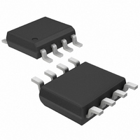
MAX941CSA+ Maxim Integrated Products, MAX941CSA+ Datasheet - Page 6

MAX941CSA+
Manufacturer Part Number
MAX941CSA+
Description
IC COMPARATOR SNGL 3V/5V 8-SOIC
Manufacturer
Maxim Integrated Products
Type
with Latchr
Datasheet
1.MAX941CSA.pdf
(14 pages)
Specifications of MAX941CSA+
Number Of Elements
1
Output Type
CMOS, Push-Pull, TTL
Voltage - Supply
2.7 V ~ 5.5 V
Mounting Type
Surface Mount
Package / Case
8-SOIC (0.154", 3.90mm Width)
Number Of Channels
1 Channel
Supply Voltage (max)
5 V
Supply Voltage (min)
3 V
Supply Current (max)
700 uA
Maximum Operating Temperature
+ 70 C
Mounting Style
SMD/SMT
Minimum Operating Temperature
0 C
Propagation Delay Time
80 ns
Comparator Type
High Speed
No. Of Comparators
1
Response Time
80ns
Ic Output Type
CMOS, TTL
Supply Current
430µA
Supply Voltage Range
2.7V To 5.5V
Amplifier Case Style
SOIC
Rohs Compliant
Yes
Lead Free Status / RoHS Status
Lead free / RoHS Compliant
High-Speed, Low-Power, 3V/5V, Rail-to-Rail,
Single-Supply Comparators
(V+ = 3.0V, T
6
_____________________________Typical Operating Characteristics (continued)
______________________________________________________________Pin Description
MAX941
_______________________________________________________________________________________
—
—
—
—
—
—
—
—
—
—
—
—
1
6
2
3
4
5
7
8
GND
V
V
OD
OS
V+
V+
2
20ns/div
A
MAX942
= +25°C, unless otherwise noted.)
PIN
—
—
—
—
—
—
—
—
—
—
—
—
1
2
3
8
5
6
7
4
PROPAGATION DELAY (t
MAX944
t
PD+
10
11
12
13
14
—
—
—
—
—
—
1
2
3
4
5
6
7
8
9
L
—
NAME
INPUT STEP = 100mV
OUTB
OUTC
OUTD
S
OUTA
—
INA+
INB+
INC+
IND+
GND
INA-
INB-
INC-
IND-
A
OUT
N.C.
—
PD+
IN+
H
V+
IN-
—
T
—
D
—
C
—
)
N
–
H
–
V
OD
MAX941 TOC18
= +5mV
Comparator A Output
Comparator A Inverting Input
Comparator A Noninverting Input
Positive Supply (V+ to GND must be ≤ 6.5V)
Comparator B Noninverting Input
Comparator B Inverting Input
Comparator B Output
Comparator C Output
Comparator C Inverting Input
Comparator C Noninverting Input
Ground
Comparator D Noninverting Input
Comparator D Inverting Input
Comparator D Output
Noninverting Input
Inverting Input
Shutdown: MAX941 is active when S
when S
The output is latched when L
is high.
Comparator Output
No Connection. Not internally connected.
INPUT
50mV/div
OUTPUT
1V/div
—
H
—
D
—
N
–
is driven low.
GND
V
V
V+
OS
OD
V+
2
—
20ns/div
A
—
T
—
C
—
H
FUNCTION
–
—
is low. The latch is transparent when L
H
PROPAGATION DELAY (t
—
D
—
N
–
is driven high; MAX941 is in shutdown
t
PD-
INPUT STEP = 100mV
PD-
)
V
OD
MAX941 TOC19
= -5mV
INPUT
50mV/div
OUTPUT
1V/div
—
A
—
T
—
C
—
H
–


