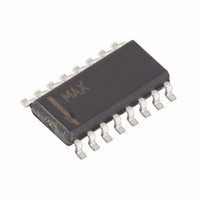
MAX984ESE+ Maxim Integrated Products, MAX984ESE+ Datasheet - Page 9

MAX984ESE+
Manufacturer Part Number
MAX984ESE+
Description
IC COMPARATOR OD 16-SOIC
Manufacturer
Maxim Integrated Products
Type
with Voltage Referencer
Datasheet
1.MAX983EPA.pdf
(17 pages)
Specifications of MAX984ESE+
Number Of Elements
4
Output Type
Open Drain
Voltage - Supply
2.5 V ~ 11 V, ±1.25 V ~ 5.5 V
Mounting Type
Surface Mount
Package / Case
16-SOIC (0.154", 3.90mm Width)
Lead Free Status / RoHS Status
Lead free / RoHS Compliant
The MAX971–MAX974/MAX981–MAX984 comprise
various combinations of a micropower 1.182V reference
and micropower comparators. The Typical Operating
Circuit shows the MAX971/MAX981 configuration, and
Figures 1a–1d show the MAX9_2–MAX9_4 configurations.
Internal hysteresis in the MAX9_1, MAX982, and
MAX9_3 provides the easiest method for implementing
hysteresis. It also produces faster hysteresis action and
consumes much less current than circuits using external
positive feedback.
Figure 1a. MAX972 Functional Diagram
Figure 1b. MAX982 Functional Diagram
1 (A1)
2 (C2)
3 (C1)
4 (B1)
1
2
3
4
( ) BUMPS FOR THE UCSP
OUTA
V-
INA+
INB+
OUTA
V-
INA+
INA-
_______________________________________________________________________________________
V-
Detailed Description
MAX982
MAX972
OUTB
OUTB
HYST
Single/Dual-Supply Comparators
INB+
INB-
REF
V+
V+
8
7
6
5
8 (A3)
7 (A2)
6 (C3)
5 (B3)
Ultra-Low-Power, Open-Drain,
This family of devices operates from a single 2.5V to 11V
power supply. The MAX9_1 and MAX9_4 have a
separate ground for the output driver, allowing operation
with dual supplies ranging from ±1.25V to ±5.5V.
Connect V- to GND when operating the MAX9_1 or
MAX9_4 from a single supply. The maximum total supply
voltage in this case is still 11V.
For proper comparator operation, the input signal can
range from the negative supply (V-) to within one volt of
the positive supply (V+ - 1V). The guaranteed common-
mode input voltage range extends from V- to (V+ -
1.3V). The inputs can be taken above and below the
supply rails by up to 300mV without damage.
Figure 1c. MAX973/MAX983 Functional Diagram
(Window Comparator)
Figure 1d. MAX974/MAX984 Functional Diagram
Power-Supply and Input Signal Ranges
1
2
3
4
1
5
6
7
8
2
3
4
OUTB
OUTA
V+
INA-
INA+
INB-
INB+
REF
OUTA
V-
INA+
INB-
V-
MAX9_4
MAX9_3
OUTC
OUTD
OUTB
HYST
IND+
INC+
GND
IND-
INC-
REF
V+
V-
16
15
14
13
12
11
10
9
8
7
6
5
9


