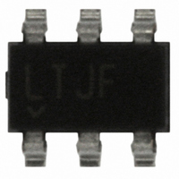
LT1719IS6#TRMPBF Linear Technology, LT1719IS6#TRMPBF Datasheet - Page 15

LT1719IS6#TRMPBF
Manufacturer Part Number
LT1719IS6#TRMPBF
Description
IC COMP R-RINOUT SINGLE SOT23-6
Manufacturer
Linear Technology
Series
UltraFast™r
Type
General Purposer
Specifications of LT1719IS6#TRMPBF
Number Of Elements
1
Output Type
CMOS, Rail-to-Rail, TTL
Voltage - Supply
2.7 V ~ 6 V
Mounting Type
Surface Mount
Package / Case
SOT-23-6
Comparator Type
General Purpose
No. Of Comparators
1
Response Time
4.5ns
Ic Output Type
CMOS, TTL
Output Compatibility
CMOS, TTL
Supply Current
4.6mA
Supply Voltage Range
2.7V To 6V
Rohs Compliant
Yes
Lead Free Status / RoHS Status
Lead free / RoHS Compliant
Other names
LT1719IS6#TRMPBFTR
Available stocks
Company
Part Number
Manufacturer
Quantity
Price
APPLICATIONS
Speed Limits
The LT1719 comparator is intended for high speed appli-
cations, where it is important to understand a few limita-
tions. These limitations can roughly be divided into three
categories: input speed limits, output speed limits, and
internal speed limits.
There are no significant input speed limits except the
shunt capacitance of the input nodes. If the 2pF typical
input nodes are driven, the LT1719 will respond.
The output speed is constrained by two mechanisms, the
first of which is the slew currents available from the output
transistors. To maintain low power quiescent operation,
the LT1719 output transistors are sized to deliver 25mA to
45mA typical slew currents. This is sufficient to drive small
capacitive loads and logic gate inputs at extremely high
speeds. But the slew rate will slow dramatically with heavy
capacitive loads. Because the propagation delay (t
definition ends at the time the output voltage is halfway
between the supplies, the fixed slew current makes the
LT1719 faster at 3V than 5V with large capacitive loads and
sufficient input overdrive.
Another manifestation of this output speed limit is skew,
the difference between t
the LT1719 vary with the process variations of the PNP
and NPN transistors, for rising edges and falling edges
respectively. The typical 0.5ns skew can have either
polarity, rising edge or falling edge faster. Again, the skew
will increase dramatically with heavy capacitive loads.
A separate output speed limit is the clamp turnaround. The
LT1719 output is optimized for fast initial response, with
some loss of turnaround speed, limiting the toggle fre-
quency. The output transistors are idled in a low power
state once V
clamp action. It is only when the output has slewed from
the old voltage to the new voltage, and the clamp circuitry
has settled, that the idle state is reached and the LT1719
is fully ready to toggle again. This is typically 8ns for each
direction, resulting in a maximum toggle frequency of
62.5MHz. With higher frequencies, dropout and runt pulses
can result. Increases in capacitive load will increase the
OH
or V
OL
U
is reached, by detecting the Schottky
PD
INFORMATION
U
+
and t
PD
–
W
. The slew currents of
U
PD
)
time needed for slewing due to the limited slew currents
and the maximum toggle frequency will decrease further.
For high toggle frequency applications, consider the
LT1394, whose linear output stage can toggle at 100MHz
typical.
The internal speed limits manifest themselves as disper-
sion. All comparators have some degree of dispersion,
defined as a change in propagation delay versus input
overdrive. The propagation delay of the LT1719 will vary
with overdrive, from a typical of 4.5ns at 20mV overdrive
to 7ns at 5mV overdrive (typical). The LT1719’s primary
source of dispersion is the hysteresis stage. As a change
of polarity arrives at the gain stage, the positive feedback
of the hysteresis stage subtracts from the overdrive avail-
able. Only when enough time has elapsed for a signal to
propagate forward through the gain stage, backwards
through the hysteresis path and forward through the gain
stage again, will the output stage receive the same level of
overdrive that it would have received in the absence of
hysteresis.
The LT1719S8 is several hundred picoseconds faster
when V
is due to the internal speed limit; the gain stage operates
between V
voltage bias due to reduced silicon junction capacitances.
In many applications, as shown in the following examples,
there is plenty of input overdrive. Even in applications
providing low levels of overdrive, the LT1719 is fast
enough that the absolute dispersion of 2.5ns (= 7 – 4.5) is
often small enough to ignore.
The gain and hysteresis stage of the LT1719 is simple,
short and high speed to help prevent parasitic oscillations
while adding minimum dispersion. This internal “self-latch”
can be usefully exploited in many applications because it
occurs early in the signal chain, in a low power, fully
differential stage. It is therefore highly immune to distur-
bances from other parts of the circuit, such as the output,
or on the supply lines. Once a high speed signal trips the
hysteresis, the output will respond, after a fixed propaga-
tion delay, without regard to these external influences
that can cause trouble in nonhysteretic comparators.
EE
= – 5V, relative to single supply operation. This
EE
and + V
S
, and it is faster with higher reverse
LT1719
15


