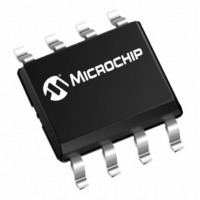
MCP6567T-E/MS Microchip Technology, MCP6567T-E/MS Datasheet - Page 17

MCP6567T-E/MS
Manufacturer Part Number
MCP6567T-E/MS
Description
IC COMP DUAL 1.8V OD 8-MSOP
Manufacturer
Microchip Technology
Type
General Purposer
Specifications of MCP6567T-E/MS
Number Of Elements
2
Output Type
CMOS, Open-Drain
Voltage - Supply
1.8 V ~ 5.5 V
Mounting Type
Surface Mount
Package / Case
8-TSSOP, 8-MSOP (0.118", 3.00mm Width)
Lead Free Status / RoHS Status
Lead free / RoHS Compliant
Other names
MCP6567T-E/MSTR
Available stocks
Company
Part Number
Manufacturer
Quantity
Price
Company:
Part Number:
MCP6567T-E/MS
Manufacturer:
MICROCHIP
Quantity:
12 000
Part Number:
MCP6567T-E/MS
Manufacturer:
MICROCHIP/微芯
Quantity:
20 000
4.0
The MCP6566/6R/6U/7/9 family of open-drain output
comparators
state-of-the-art CMOS process. They are suitable for a
wide range of high speed applications requiring low-
power consumption.
4.1
4.1.1
The input stage of this family of devices uses two
differential input stages in parallel. This configuration
provides three regions of operation, one operates at
low input voltages, one at high input voltages, and one
at mid input voltage. With this topology, the input
voltage range is 0.3V above V
while providing low offset voltage throughout the
common mode range. The input offset voltage is
measured at both V
proper operation.
The MCP6566/6R/6U/7/9 family has internally-set
hysteresis
offset accuracy and large enough to eliminate output
chattering caused by the comparator’s own input noise
voltage
offset voltage (V
(input-referred) low-high and high-low trip points. Input
hysteresis voltage (V
the same trip points.
FIGURE 4-1:
comparators’ internal hysteresis eliminates
output chatter caused by input noise voltage.
2011 Microchip Technology Inc.
-1
-2
-3
8
7
6
5
4
3
2
1
0
E
V
APPLICATIONS INFORMATION
Comparator Inputs
DD
NI
V
.
NORMAL OPERATION
HYST
= 5.0V
V
OUT
Figure 4-1
are
that is small enough to maintain input
OS
SS
) is the center (average) of the
Time (100 ms/div)
HYST
- 0.3V and V
The MCP6566/6R/6U/7/9
fabricated
depicts this behavior. Input
) is the difference between
Hysteresis
DD
V
IN
and 0.3V below V
–
DD
on
+ 0.3V to ensure
Microchip’s
25
20
15
10
5
0
-5
-10
-15
-20
-25
-30
SS
,
4.1.2
The ESD protection on the inputs can be depicted as
shown in
protect the input transistors, and to minimize input bias
current (I
when they try to go more than one diode drop below
V
above V
allow normal operation, and low enough to bypass ESD
events within the specified limits.
FIGURE 4-2:
Structures.
In order to prevent damage and/or improper operation
of these amplifiers, the circuits they are in must limit the
currents (and voltages) at the V
Section 1.1 “Maximum Ratings*”
Section 1.0 “Electrical
shows the recommended approach to protecting these
inputs. The internal ESD diodes prevent the input pins
(V
the resistors R
out of the input pin. Diodes D
pin (V
When implemented as shown, resistors R
limit the current through D
FIGURE 4-3:
Inputs.
SS
IN
MCP6566/6R/6U/7/9
V
V
. They also clamp any voltages that go too far
+ and V
V
V
1
2
V
IN
IN
DD
SS
+
R
R
+ and V
DD
B
1
2
). The input ESD diodes clamp the inputs
Figure
; their breakdown voltage is high enough to
Bond
Bond
Bond
R
R
INPUT VOLTAGE AND CURRENT
LIMITS
Pad
Pad
Pad
IN
1
2
D
V
V
–) from going too far below ground, and
1
1
SS
SS
and R
D
IN
4-2. This structure was chosen to
– (minimum expected V
– (minimum expected V
2
–) from going too far above V
2
Simplified Analog Input ESD
Protecting the Analog
limit the possible current drawn
Stage
Input
Characteristics”).
MCP656X
2 mA
2 mA
1
+
–
and D
R
1
V
3
and D
DD
IN
+ and V
2
.
at the beginning of
2
DS22143C-page 17
V
Bond
prevent the input
Pad
PU
R
1
IN
2
1
)
and R
4
)
– pins (see
Figure 4-3
V
V
IN
OUT
–
2
also
DD
.


