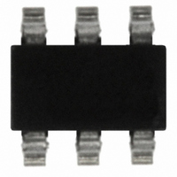
LT1719CS6#TRMPBF Linear Technology, LT1719CS6#TRMPBF Datasheet - Page 10

LT1719CS6#TRMPBF
Manufacturer Part Number
LT1719CS6#TRMPBF
Description
IC COMP R-RINOUT SINGLE SOT23-6
Manufacturer
Linear Technology
Series
UltraFast™r
Type
General Purposer
Specifications of LT1719CS6#TRMPBF
Number Of Elements
1
Output Type
CMOS, Rail-to-Rail, TTL
Voltage - Supply
2.7 V ~ 6 V
Mounting Type
Surface Mount
Package / Case
SOT-23-6
Comparator Type
General Purpose
No. Of Comparators
1
Response Time
4.5ns
Ic Output Type
CMOS, TTL
Output Compatibility
CMOS, TTL
Supply Current
4.6mA
Supply Voltage Range
2.7V To 6V
Rohs Compliant
Yes
Lead Free Status / RoHS Status
Lead free / RoHS Compliant
Other names
LT1719CS6#TRMPBFTR
Available stocks
Company
Part Number
Manufacturer
Quantity
Price
APPLICATIONS
LT1719
10
shutdown is active high, this resistor adds little power
drain during shutdown. A logic high disables the compara-
tor. The LT1719S8 logic interface is based on the output
power rails, + V
For applications that do not use the shutdown feature, it
may be helpful to tie the shutdown control to ground
through a 100 resistor rather than directly. This allows
the SHDN pin to be pulled high during debug or in-circuit
test (bed of nails) so that the output node can be wiggled
without damaging the low impedance output driver of the
LT1719.
The shutdown state is not guaranteed to be useful as a
multiplexer. Digital signals can have extremely fast edge
rates that may be enough to momentarily activate the
LT1719 output stage via internal capacitive coupling. No
damage to the LT1719 will result, but this could prove
deleterious to the intended recipient of the signal.
The LT1719 includes a FET pull-up on the shutdown
control pin (see Simplified Schematic) as well as other
internal structures to make the shutdown state current
drain <<1 A. Shutdown is guaranteed with an open circuit
on the shutdown control pin. When the shutdown control
pin is driven to + V
impedance of the pull-up FET will cause a current flow of
7 A (typ) into the +V
Currents in all other power supply terminals will be <1 A.
Power Supply Sequencing
The LT1719S8 is designed to tolerate any power supply
sequencing at system turn-on and power down. In any of
the previously shown power supply configurations, the
various supplies can activate in any order without exces-
sive current drain by the LT1719.
As always, the Absolute Maximum Ratings must not be
exceeded, either on the power supply terminals or the
input terminals. Power supply sequencing problems can
occur when input signals are powered from supplies that
are independent of the LT1719’s supplies. For the com-
parator inputs, the signals should be powered from the
same V
down input, the signal should be powered from the same
+V
S
as the LT1719.
CC
and V
S
EE
and GND.
supplies as the LT1719. For the shut-
U
S
/V
S
/V
+
INFORMATION
+
– 0.5V, the 70k linear region
U
pin and out the shutdown pin.
W
U
Hysteresis
The LT1719 includes internal hysteresis, which makes it
easier to use than many other similar speed comparators.
The input-output transfer characteristic is illustrated in
Figure 3 showing the definitions of V
upon the two measurable trip points. The hysteresis band
makes the LT1719 well behaved, even with slowly moving
inputs.
The exact amount of hysteresis will vary from part to part
as indicated in the specifications table. The hysteresis
level will also vary slightly with changes in supply voltage
and common mode voltage. A key advantage of the
LT1719 is the significant reduction in these effects, which
is important whenever an LT1719 is used to detect a
threshold crossing in one direction only. In such a case,
the relevant trip point will be all that matters, and a stable
offset voltage with an unpredictable level of hysteresis, as
seen in competing comparators, is useless. The LT1719 is
many times better than prior comparators in these re-
gards. In fact, the CMRR and PSRR tests are performed by
checking for changes in either trip point to the limits
indicated in the specifications table. Because the offset
voltage is the average of the trip points, the CMRR and
PSRR of the offset voltage is therefore guaranteed to be at
least as good as those limits. This more stringent test also
puts a limit on the common mode and power supply
dependence of the hysteresis voltage.
V
OL
Figure 3. Hysteresis I/O Characteristics
V
TRIP
V
OS
–
=
0
V
(= V
TRIP
TRIP
+
+ V
2
V
HYST
+
TRIP
– V
TRIP
–
V
HYST
–
)
/2
V
TRIP
OS
+
and V
V
IN
V
OH
= V
1719 F03
HYST
IN
+
– V
IN
based
–


