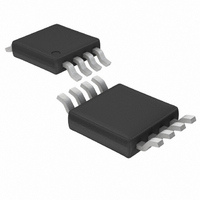
LT1671CMS8 Linear Technology, LT1671CMS8 Datasheet - Page 6

LT1671CMS8
Manufacturer Part Number
LT1671CMS8
Description
IC COMPARATOR 60NS LOW PWR 8MSOP
Manufacturer
Linear Technology
Type
with Latchr
Datasheet
1.LT1671CS8PBF.pdf
(12 pages)
Specifications of LT1671CMS8
Number Of Elements
1
Output Type
CMOS, Complementary, TTL
Mounting Type
Surface Mount
Package / Case
8-TSSOP, 8-MSOP (0.118", 3.00mm Width)
Lead Free Status / RoHS Status
Contains lead / RoHS non-compliant
Available stocks
Company
Part Number
Manufacturer
Quantity
Price
Company:
Part Number:
LT1671CMS8
Manufacturer:
LT
Quantity:
10 000
Company:
Part Number:
LT1671CMS8#PBF
Manufacturer:
LT
Quantity:
920
Part Number:
LT1671CMS8#PBF
Manufacturer:
LINEAR/凌特
Quantity:
20 000
Company:
Part Number:
LT1671CMS8#TRPBF
Manufacturer:
LT
Quantity:
2 190
Part Number:
LT1671CMS8#TRPBF
Manufacturer:
LINEAR/凌特
Quantity:
20 000
PIN
LT1671
V
+IN (Pin 2): Noninverting Input.
–IN (Pin 3): Inverting Input.
V
or – 5V.
LATCH ENABLE (Pin 5): Latch Control Pin. When high, the
outputs remain in a latched condition, independent of the
current state of the inputs.
TYPICAL PERFORMANCE CHARACTERISTICS
TI I G DIAGRA S
6
+
–
U
W
V
(Pin 1): Positive Supply Voltage. Normally 5V.
(Pin 4): Negative Supply Voltage. Normally either 0V
OUT
V
IN
FUNCTIONS
U
+IN
– 95mV
5mV
U
t
5mV Overdrive
V
V
PD
S
OD
V
= 5V
+
IN
= 5mV
Response Time to
U
V
OD
20ns/DIV
W
W
t
PD
U
1671 G18
1.4V
Q OUT
0V
1671 TD01
GND (Pin 6): Ground.
Q OUT (Pin 7): Noninverting Logic Output. This pin is high
when +IN is above – IN and LATCH ENABLE is low.
Q OUT (Pin 8): Inverting Logic Output. This pin is low
when +IN is above – IN and LATCH ENABLE is low.
ENABLE
LATCH
V
OUT
V
IN
+IN
– 95mV
5mV
t
5mV Overdrive
V
V
PD
S
OD
= 5V
–
= 5mV
Response Time to
t
SU
20ns/DIV
t
PD
t
H
1671 G19
1.4V
Q OUT
0V
1671 TD02


