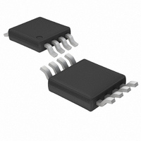
LT1711CMS8#TRPBF Linear Technology, LT1711CMS8#TRPBF Datasheet - Page 7

LT1711CMS8#TRPBF
Manufacturer Part Number
LT1711CMS8#TRPBF
Description
IC COMP R-RINOUT SINGLE 8-MSOP
Manufacturer
Linear Technology
Series
UltraFast™r
Type
General Purposer
Datasheet
1.LT1711CMS8PBF.pdf
(12 pages)
Specifications of LT1711CMS8#TRPBF
Number Of Elements
1
Output Type
CMOS, Complementary, Rail-to-Rail, TTL
Voltage - Supply
2.4 V ~ 12 V, ±2.4 V ~ 6 V
Mounting Type
Surface Mount
Package / Case
8-TSSOP, 8-MSOP (0.118", 3.00mm Width)
Lead Free Status / RoHS Status
Lead free / RoHS Compliant
Available stocks
Company
Part Number
Manufacturer
Quantity
Price
APPLICATIO S I FOR ATIO
PI FU CTIO S
Common Mode Considerations
The LT1711/LT1712 are specified for a common mode
range of – 5.1V to 5.1V on a 5V supply, or a common
mode range of – 0.1V to 5.1V on a single 5V supply. A more
general consideration is that the common mode range is
from 100mV below the negative supply to 100mV above
the positive supply, independent of the actual supply
voltage. The criteria for common mode limit is that the
output still responds correctly to a small differential input
signal.
When either input signal falls outside the common mode
limit, the internal PN diode formed with the substrate can
turn on resulting in significant current flow through the
die. Schottky clamp diodes between the inputs and the
supply rails speed up recovery from excessive overdrive
conditions by preventing these substrate diodes from
turning on.
Input Bias Current
Input bias current is measured with the outputs held at
2.5V with a 5V supply voltage. As with any rail-to-rail
LT1712
– IN A (Pin 1): Inverting Input of A Channel Comparator.
+ IN A (Pin 2): Noninverting Input of A Channel
Comparator.
V
3 and 6 should be connected together externally.
V
4 and 5 should be connected together externally.
+ IN B (Pin 7): Noninverting Input of B Channel
Comparator.
– IN B (Pin 8): Inverting Input of B Channel Comparator.
LATCH ENABLE B (Pin 9): Latch Enable Input of B Channel
Comparator. With a logic high, the B output is latched.
GND (Pin 10): Ground Supply Voltage of B Channel
Comparator, Usually 0V.
–
+
U
(Pins 3, 6): Negative Supply Voltage, Usually – 5V. Pins
(Pins 4, 5): Positive Supply Voltage, Usually 5V. Pins
U
U
U
U
W
U
Q B (Pin 11): Noninverting Output of B Channel
Comparator.
Q B (Pin 12): Inverting Output of B Channel
Comparator.
Q A (Pin 13): Inverting Output of A Channel
Comparator.
Q A (Pin 14): Noninverting Output of A Channel
Comparator.
GND (Pin 15): Ground Supply Voltage of A Channel
Comparator, Usually 0V
LATCH ENABLE A (Pin 16): Latch Enable Input of A
Channel Comparator. With a logic high, the A output is
latched.
differential input stage, the LT1711/LT1712 bias current
flows into or out of the device depending upon the com-
mon mode level. The input circuit consists of an NPN pair
and a PNP pair. For inputs near the negative rail, the NPN
pair is inactive, and the input bias current flows out of the
device; for inputs near the positive rail, the PNP pair is
inactive, and these currents flow into the device. For inputs
far enough away from the supply rails, the input bias
current will be some combination of the NPN and PNP bias
currents. As the differential input voltage increases, the
input current of each pair will increase for one of the inputs
and decrease for the other input. Large differential input
voltages result in different input currents as the input
stage enters various regions of operation. To reduce the
influence of these changing input currents on system
operation, use a low source resistance.
Latch Pin Dynamics
The internal latches of the LT1711/LT1712 comparators
retain the input data (output latched) when their respec-
tive latch pin goes high. The latch pin will float to a low
state when disconnected, but it is better to ground the
LT1711/LT1712
7


